参数资料
| 型号: | AD625KNZ |
| 厂商: | Analog Devices Inc |
| 文件页数: | 6/15页 |
| 文件大小: | 0K |
| 描述: | IC AMP INST 25MHZ LN 16DIP |
| 标准包装: | 25 |
| 放大器类型: | 仪表 |
| 电路数: | 1 |
| 转换速率: | 5 V/µs |
| 增益带宽积: | 25MHz |
| -3db带宽: | 650kHz |
| 电流 - 输入偏压: | 20nA |
| 电压 - 输入偏移: | 25µV |
| 电流 - 电源: | 3.5mA |
| 电压 - 电源,单路/双路(±): | ±6 V ~ 18 V |
| 工作温度: | 0°C ~ 70°C |
| 安装类型: | 通孔 |
| 封装/外壳: | 16-DIP(0.300",7.62mm) |
| 供应商设备封装: | 16-PDIP |
| 包装: | 管件 |
| 产品目录页面: | 770 (CN2011-ZH PDF) |
AD625
REV. D
–14–
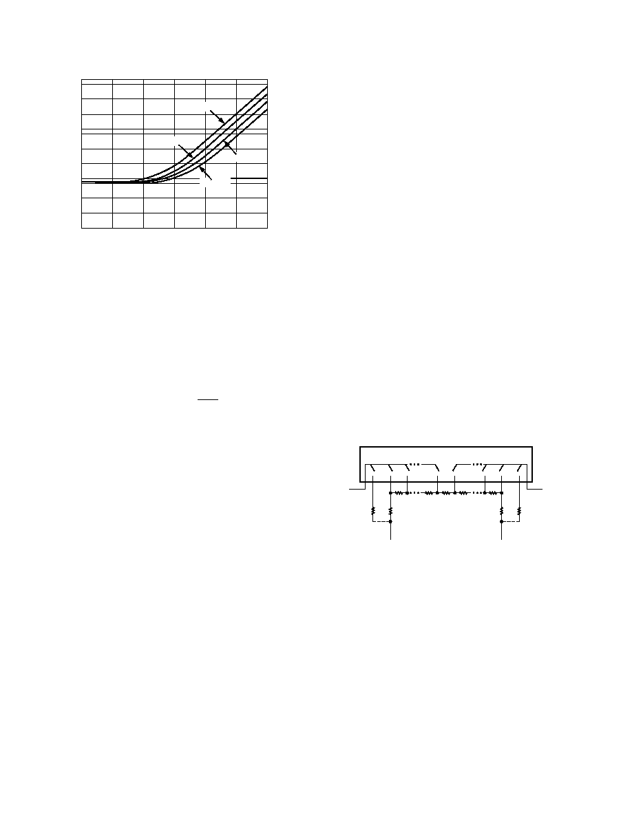
GAIN
1000
1
SETTLING
TIME
–
s
800
400
200
100
80
40
20
10
8
4
2
1
4
16
64
256
1024
4096
RON = 1k
RON = 500
RON = 200
RON = 0
Figure 40. Time to 0.01% of a 20 V Step Input for
SPGA with AD625
DETERMINING SPGA RESISTOR NETWORK VALUES
The individual resistors in the gain network can be calculated
sequentially using the formula given below. The equation deter-
mines the resistors as labeled in Figure 41. The feedback resis-
tors and the gain setting resistors are interactive, therefore; the
formula must be a series where the present term is dependent on
the preceding term(s). The formula
Rk
R
G
R
Fi
Fj
j
i
F
+
=
∑
1
0
1
0
20
1
0
(
–
)( –
)
can be used to calculate the necessary feedback resistors for any
set of gains. This formula yields a network with a total resistance
of 40 k
. A dummy variable (j) serves as a counter to keep a
running total of the preceding feedback resistors. To illustrate
how the formula can be applied, an example similar to the
calculation used for the resistor network in Figure 38 is exam-
ined below.
1) Unity gain is treated as a separate case. It is implemented
with separate 20 k
feedback resistors as shown in Figure 41.
It is then ignored in further calculations.
2) Before making any calculations it is advised to draw a resistor
network similar to the network in Figure 41. The network
will have (2
× M) + 1 resistors, where M = number of gains.
For Figure 38 M = 3 (4, 16, 64), therefore, the resistor string
will have seven resistors (plus the two 20 k
“side” resistors
for unity gain).
3) Begin all calculations with G0 = 1 and RF
0
= 0.
RF
1
= (20 k
– R
F0) (1–1/4): RF0 = 0 ∴ RF1 = 15 k
RF
2
= [20 k
– (R
F0 + RF1)] (1–4/16):
RF
0
+ RF
1
= 15 k
∴ R
F2 = 3.75 k
RF
3
= [20 k
– (R
F0 + RF1 + RF2)] (1–16/64):
RF
0
+ RF
1
+ RF
2
= 18.75 k
∴ R
F3 = 937.5
4) The center resistor (RG of the highest gain setting), is deter-
mined last. Its value is the remaining resistance of the 40 k
string, and can be calculated with the equation:
Rk
R
GFj
j
M
=
∑
(
–
)
40
2
0
RG = 40 k
– 2 (R
F0 + RF1 + RF2 + RF3 )
40 k
– 39.375 k = 625
5) If different resistor values are desired, all the resistors in the
network can be scaled by some convenient factor. However,
raising the impedance will increase the RTO errors, lowering
the total network resistance below 20 k
can result in ampli-
fier instability. More information on this phenomenon is
given in the RPGA section of the data sheet. The scale factor
will not affect the unity gain feedback resistors. The resistor
network in Figure 38 has a scaling factor of 650/625 = 1.04,
if this factor is used on RF
1
, RF
2
, RF
3
, and RG, then the resis-
tor values will match exactly.
6) Round off errors can be cumulative, therefore, it is advised to
carry as many significant digits as possible until all the values
have been calculated.
AD75xx
TO GAIN SENSE
(PIN 2)
20k
RF1
20k
RF2
RFN
RFG
RFN
RF2
TO GAIN SENSE
(PIN 15)
TO GAIN DRIVE
(PIN 5)
TO GAIN DRIVE
(PIN 12)
CONNECT IF UNITY
GAIN IS DESIRED
CONNECT IF UNITY
GAIN IS DESIRED
Figure 41. Resistors for a Gain Setting Network
相关PDF资料 |
PDF描述 |
|---|---|
| TSW-109-05-G-S | CONN HEADER 9POS .100" SGL GOLD |
| AD526ADZ | IC AMP PGA 10MA 16CDIP |
| 53324-0560 | CONN HEADER 2MM 5POS PCB TIN |
| OP470EY | IC OPAMP GP 6MHZ QUAD LN 14CDIP |
| 929836-02-04-RK | CONN HEADER .100 DUAL STR 8POS |
相关代理商/技术参数 |
参数描述 |
|---|---|
| AD625KNZ | 制造商:Analog Devices 功能描述:IC AMP GAIN |
| AD625S | 制造商:AD 制造商全称:Analog Devices 功能描述:Programmable Gain Instrumentation Amplifier |
| AD625SCHIPS | 制造商:AD 制造商全称:Analog Devices 功能描述:Programmable Gain Instrumentation Amplifier |
| AD625SD | 功能描述:IC AMP INST 25MHZ LN 16CDIP RoHS:否 类别:集成电路 (IC) >> Linear - Amplifiers - Instrumentation 系列:- 其它有关文件:TS1854A View All Specifications 标准包装:50 系列:- 放大器类型:通用 电路数:4 输出类型:满摆幅 转换速率:0.25 V/µs 增益带宽积:630kHz -3db带宽:- 电流 - 输入偏压:16nA 电压 - 输入偏移:1000µV 电流 - 电源:162µA 电流 - 输出 / 通道:48mA 电压 - 电源,单路/双路(±):1.8 V ~ 6 V 工作温度:-40°C ~ 125°C 安装类型:表面贴装 封装/外壳:14-SOIC(0.154",3.90mm 宽) 供应商设备封装:14-SO 包装:管件 |
| AD625SD/883 | 制造商:Analog Devices 功能描述: |
发布紧急采购,3分钟左右您将得到回复。