参数资料
| 型号: | AD641AP-REEL7 |
| 厂商: | Analog Devices Inc |
| 文件页数: | 14/16页 |
| 文件大小: | 0K |
| 描述: | IC AMP LOG LP 2.3MA 20PLCC |
| 标准包装: | 250 |
| 放大器类型: | 对数 |
| 电路数: | 1 |
| -3db带宽: | 250MHz |
| 电流 - 输入偏压: | 7µA |
| 电压 - 输入偏移: | 50µV |
| 电流 - 电源: | 35mA |
| 电流 - 输出 / 通道: | 2.3mA |
| 电压 - 电源,单路/双路(±): | ±4.5 V ~ 7.5 V |
| 工作温度: | -40°C ~ 85°C |
| 安装类型: | 表面贴装 |
| 封装/外壳: | 20-LCC(J 形引线) |
| 供应商设备封装: | 20-PLCC(9x9) |
| 包装: | 带卷 (TR) |
REV. C
AD641
–7–
Transistors Q3 through Q6 form the full wave detector, whose
output is buffered by the cascodes Q9 and Q10. For zero input
Q3 and Q5 conduct only a small amount (a total of about 32
A)
of the 565
A tail currents supplied to pairs Q3–Q4 and Q5–Q6.
This “pedestal” current flows in output cascode Q9 to the LOG
OUT node (Pin 14). When driven to the peak output of the
preceding stage, Q3 or Q5 (depending on signal polarity) con-
ducts most of the tail current, and the output rises to 532
A.
The LOG OUT current has thus changed by 500
A as the
input has changed from zero to its maximum value. Since the
detectors are spaced at 10 dB intervals, the output increases by
50
A/dB, or 1 mA per decade. This scaling parameter is trimmed
to absolute accuracy using a 2 kHz square wave. At frequencies
near the system bandwidth, the slope is reduced due to the
reduced output of the limiter stages, but it is still relatively in-
sensitive to temperature variations so that a simple external
slope adjustment can restore scaling accuracy.
The intercept position bias generator (Figure 17) removes the
pedestal current from the summed detector outputs. It is ad-
justed during manufacture such that the output (flowing into
Pin 14) is 1 mA when a 2 kHz square-wave input of exactly
±10 mV is applied to the AD641. This places the dc intercept at
precisely 1 mV. The LOG COM output (Pin 13) is the comple-
ment of LOG OUT. It also has a 1 mV intercept, but with an
inverted slope of –1 mA/decade. Because its pedestal is very
large (equivalent to about 100 dB), its intercept voltage is not
guaranteed. The intercept positioning currents include a special
internal temperature compensation (ITC) term which can be
disabled by connecting Pin 8 to ground.
The logarithmic function of the AD641 is absolutely calibrated
to within
±0.3 dB (or ±15 A) for 2 kHz square-wave inputs of
±1 mV to ±100 mV, and to within ±1 dB between ±750 V and
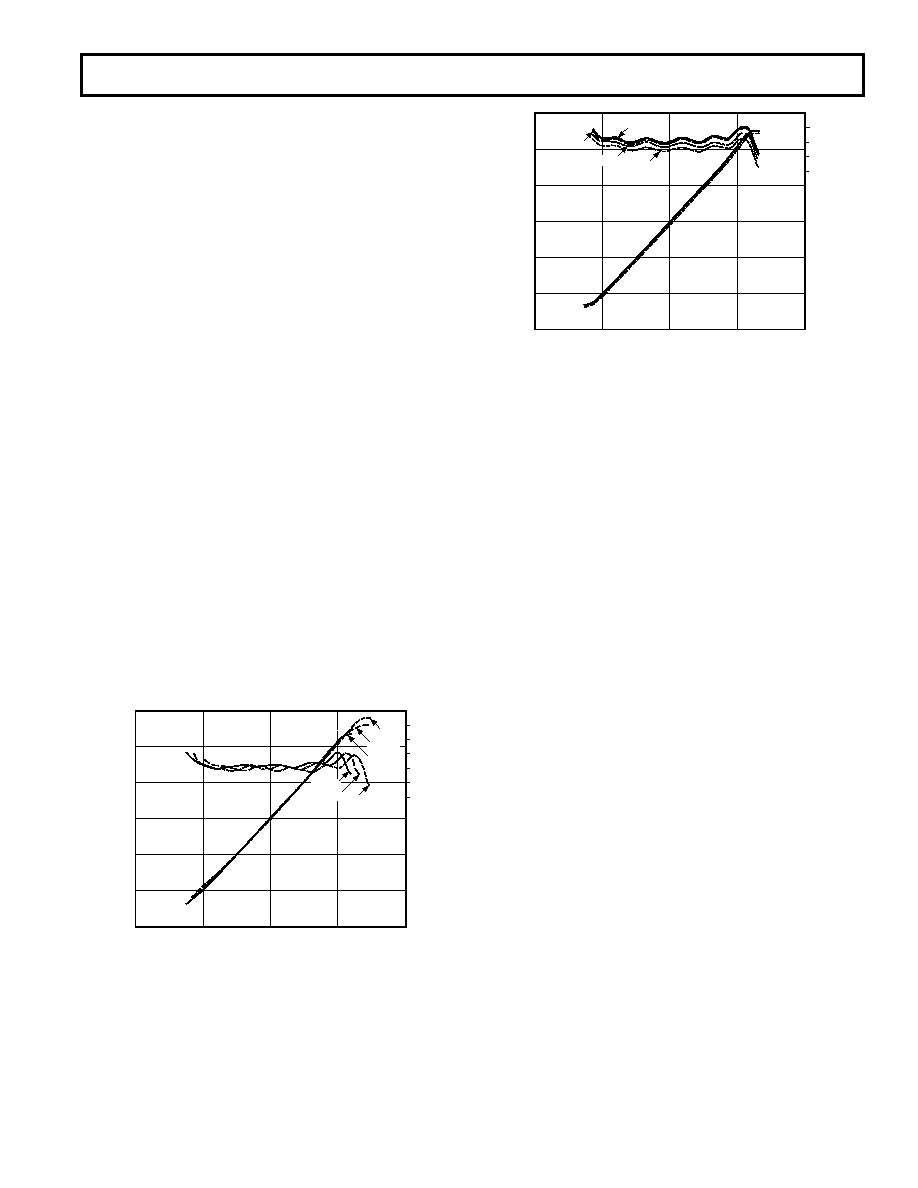
±200 mV. Figure 18 is a typical plot of the dc transfer function,
2.5
–0.5
1000.0
0.5
0
1.0
0.1
1.0
1.5
2.0
100.0
10.0
INPUT VOLTAGE – mV
OUTPUT
CURRENT
–
mA
2
1
0
–1
–2
3
ABSOLUTE
ERROR
–
dB
–55 C
+125 C
+25 C
+125 C
–55 C
+25 C
Figure 18. Logarithmic Output and Absolute Error vs. DC
or Square Wave Input at TA = –55°C, +25°C, and +125°C,
Input Direct to Pins 1 and 20
2.5
–0.5
10000
0.5
0
10
0.1
1.0
1.5
2.0
1000
100
INPUT VOLTAGE – mV
OUTPUT
CURRENT
–
mA
1
0
–1
–2
ABSOLUTE
ERROR
–
dB
+25 C
–55 C
+85 C
+125 C
Figure 19. Logarithmic Output and Absolute Error vs. DC
or Square Wave Input at TA = –55°C, +25°C, +85°C and
+125
°C. Input via On-Chip Attenuator
showing the outputs at temperatures of –55
°C, +25°C and
+125
°C. While the slope and intercept are seen to be little af-
fected by temperature, there is a lateral shift in the end points of
the “linear” region of the transfer function, which reduces the
effective dynamic range.
The on chip attenuator can be used to handle input levels 20 dB
higher, that is, from
±7.5 mV to ±2 V for dc or square wave
inputs. It is specially designed to have a positive temperature
coefficient and is trimmed to position the intercept at 10 mV dc
(or –24 dBm for a sinusoidal input) over the full temperature
range. When using the attenuator the internal bias compensa-
tion should be disabled by grounding Pin 8. Figure 19 shows
the output at –55
°C, +25°C, +85°C and +125°C for a single,
AD641 with the attenuator in use; the curves overlap almost
perfectly, and the lateral shift in the transfer function does not
occur. Therefore, the full dynamic range is available at all
temperatures.
The output of the final limiter is available in differential form at
Pins 10 and 11. The output impedance is 75
to ground from
either pin. For most input levels, this output will appear to have
roughly a square waveform. The signal path may be extended
using these outputs (see OPERATION OF CASCADED
AD641s). The logarithmic outputs from two or more AD641s
can be directly summed with full accuracy.
A pair of 1 k
applications resistors, RG1 and RG2 (Figure 17)
are accessed via Pins 15, 16 and 17. These can be used to con-
vert an output current to a voltage, with a slope of 1 V/decade
(using one resistor), 2 V/decade (both resistors in series) or
0.5 V/decade (both in parallel). Using all the resistors from two
AD641s (for example, in a cascaded configuration) ten slope
options from 0.25 V to 4 V/decade are available.
相关PDF资料 |
PDF描述 |
|---|---|
| TV02W6V0-HF | TVS 200W 6V UNIDIRECT SOD-123 |
| AD606JR-REEL7 | IC AMP LOG LP 1.2MA 16SOIC |
| AD605AR-REEL7 | IC AMP VGA DUAL LN 40MA 16SOIC |
| TV04A780J-G | TVS 400W 80V UNIDIRECT 5% SMA |
| TV02W600-G | TVS 200W 60V UNIDIRECT SOD-123 |
相关代理商/技术参数 |
参数描述 |
|---|---|
| AD641APZ | 功能描述:IC AMP LOG LP 2.3MA 20PLCC RoHS:是 类别:集成电路 (IC) >> Linear - Amplifiers - Instrumentation 系列:- 标准包装:50 系列:- 放大器类型:J-FET 电路数:2 输出类型:- 转换速率:3.5 V/µs 增益带宽积:1MHz -3db带宽:- 电流 - 输入偏压:30pA 电压 - 输入偏移:2000µV 电流 - 电源:200µA 电流 - 输出 / 通道:- 电压 - 电源,单路/双路(±):7 V ~ 36 V,±3.5 V ~ 18 V 工作温度:0°C ~ 70°C 安装类型:通孔 封装/外壳:8-DIP(0.300",7.62mm) 供应商设备封装:8-PDIP 包装:管件 |
| AD641-EB | 制造商:Analog Devices 功能描述:AD641 EVALUATION BOARD - Bulk |
| AD641N | 制造商:未知厂家 制造商全称:未知厂家 功能描述:Amplifier. Other |
| AD641P | 制造商:未知厂家 制造商全称:未知厂家 功能描述:Amplifier. Other |
| AD641Q | 制造商:未知厂家 制造商全称:未知厂家 功能描述:Amplifier. Other |
发布紧急采购,3分钟左右您将得到回复。