- 您现在的位置:买卖IC网 > PDF目录22156 > AD650AD (Analog Devices Inc)IC V-F/F-V CONV 1MHZ 14-CDIP PDF资料下载
参数资料
| 型号: | AD650AD |
| 厂商: | Analog Devices Inc |
| 文件页数: | 1/20页 |
| 文件大小: | 385K |
| 描述: | IC V-F/F-V CONV 1MHZ 14-CDIP |
| 标准包装: | 25 |
| 类型: | 电压至频率和频率至电压 |
| 频率 - 最大: | 1MHz |
| 全量程: | ±150ppm/°C |
| 线性: | ±0.1% |
| 安装类型: | 通孔 |
| 封装/外壳: | 14-CDIP(0.300",7.62mm) |
| 供应商设备封装: | 14-CDIP |
| 包装: | 管件 |
Voltage-to-Frequency and
Fre uenc-to-Volta e Converter
Data Sheet
AD650
Rev. E
Document Feedback
Information furnished by Analog Devices is believed to be accurate and reliable. However, no
responsibility is assumed by Analog Devices for its use, nor for any infringements of patents or other
rights of third parties that may result from its use. Specifications subject to change without notice. No
license is granted by implication or otherwise under any patent or patent rights of Analog Devices.
Tr mrk n r i r r mrk r h r r fh irr iv wn r
One Technology Way, P.O. Box 9106, Norwood, MA 02062-9106, U.S.A.
Tel: 781.329.4700 ?013 Analog Devices, Inc. All rights reserved.
T hni l r
www n l m
FEATURES
V/F conversion to 1 MHz
Reliable monolithic construction
Very low nonlinearity
0.002% typ at 10 kHz
0.005% typ at 100 kHz
0.07% typ at 1 MHz
Input offset trimmable to zero
CMOS- or TTL-compatible
Unipolar, bipolar, or differential V/F
V/F or F/V conversion
Available in surface mount
MIL-STD-883 compliant versions available
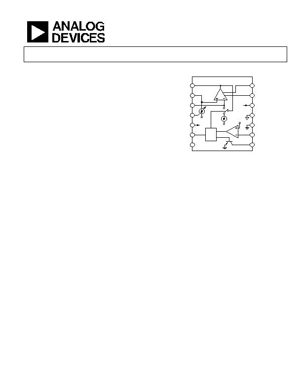
FUNCTIONAL BLOCK DIAGRAM
OP
AMP
COMP
IN
FREQ
OUT
OUT
ONE
SHOT
8 F
OUTPUT
9
COMPARATOR
INPUT
10
DIGITAL
GND
11
ANALOG
GND
12
+V
S
13
OFFSET
NULL
7
NC
6
ONE
SHOT
APACITOR
5
V
S
4
BIPOLAR
OFFSET
CURRENT
3
IN
2
+IN
1
V
OUT
14
OFFSET
NULL
INPUT
OFFSET
TRIM
0.6V
AD650
V
S
V
S
1mA
S1
NC = NO CONNECT
Figure 1.
PRODUCT DESCRIPTION
The AD650 V/F/V (voltage-to-frequency or frequency-to-voltage
converter) provides a combination of high frequency operation
and low nonlinearity previously unavailable in monolithic form.
The inherent monotonicity of the V/F transfer function makes
the AD650 useful as a high-resolution analog-to-digital converter.
A flexible input configuration allows a wide variety of input
voltage and current formats to be used, and an open-collector
output with separate digital ground allows simple interfacing to
either standard logic families or opto-couplers.
The linearity error of the AD650 is typically 20 ppm (0.002% of
full scale) and 50 ppm (0.005%) maximum at 10 kHz full scale.
This corresponds to approximately 14-bit linearity in an analog-
to-digital converter circuit. Higher full-scale frequencies or
longer count intervals can be used for higher resolution
conversions. The AD650 has a useful dynamic range of six
decades allowing extremely high resolution measurements.
Even at 1 MHz full scale, linearity is guaranteed less than
1000 ppm (0.1%) on the AD650KN, BD, and SD grades.
In addition to analog-to-digital conversion, the AD650 can be
used in isolated analog signal transmission applications,
phased-locked loop circuits, and precision stepper motor speed
controllers. In the F/V mode, the AD650 can be used in
precision tachometer and FM demodulator circuits.
The input signal range and full-scale output frequency are user-
programmable with two external capacitors and one resistor.
Input offset voltage can be trimmed to zero with an external
potentiometer.
The AD650JN and AD650KN are offered in plastic 14-lead DIP
packages. The AD650JP is available in a 20-lead plastic leaded
chip carrier (PLCC). Both plastic packaged versions of the
AD650 are specified for the commercial temperature range
(0癈 to 70癈). For industrial temperature range (25癈 to
+85癈) applications, the AD650AD and AD650BD are offered
in ceramic packages. The AD650SD is specified for the full
55癈 to +125癈 extended temperature range.
PRODUCT HIGHLIGHTS
1. Can operate at full-scale output frequencies up to 1 MHz
(in addition to having very high linearity).
2. Can be configured to accommodate bipolar, unipolar, or
differential input voltages, or unipolar input currents.
3. TTL or CMOS compatibility is achieved by using an open
collector frequency output. The pull-up resistor can be
connected to voltages up to 30 V.
4. The same components used for V/F conversion can also be
used for F/V conversion by adding a simple logic biasing
network and reconfiguring the AD650.
5. Separate analog and digital grounds prevent ground loops
in real-world applications.
6. Available in versions compliant with MIL-STD-883.
相关PDF资料 |
PDF描述 |
|---|---|
| ABB66DHRQ-S578 | CONN EDGECARD EXTEND 132POS .050 |
| EN91L5X2 | BATTERY PK 15.0V AA SIZ ALKALINE |
| AD537KH | IC V/F CONV TO-100-10 |
| 1N4004-T | RECTIFIER 400V 1A DO-41 |
| AD652KPZ | IV V-F CONVERTER SYNC 20-PLCC |
相关代理商/技术参数 |
参数描述 |
|---|---|
| AD650ADE | 制造商:Analog Devices 功能描述: |
| AD650B | 制造商:AD 制造商全称:Analog Devices 功能描述:Voltage-to-Frequency and Frequency-to-Voltage Converter |
| AD650BD | 功能描述:IC V-F/F-V CONV 1MHZ 14-CDIP RoHS:否 类别:集成电路 (IC) >> PMIC - V/F 和 F/V 转换器 系列:- 标准包装:1 系列:- 类型:频率至电压 频率 - 最大:10kHz 全量程:- 线性:±0.3% 安装类型:表面贴装 封装/外壳:8-SOIC(0.154",3.90mm 宽) 供应商设备封装:8-SOIC 包装:Digi-Reel® 其它名称:LM2917MX-8/NOPBDKR |
| AD650J | 制造商:AD 制造商全称:Analog Devices 功能描述:Voltage-to-Frequency and Frequency-to-Voltage Converter |
| AD650JN | 功能描述:IC V-F/F-V CONVERTER 14-DIP RoHS:否 类别:集成电路 (IC) >> PMIC - V/F 和 F/V 转换器 系列:- 标准包装:1 系列:- 类型:频率至电压 频率 - 最大:10kHz 全量程:- 线性:±0.3% 安装类型:表面贴装 封装/外壳:8-SOIC(0.154",3.90mm 宽) 供应商设备封装:8-SOIC 包装:Digi-Reel® 其它名称:LM2917MX-8/NOPBDKR |
发布紧急采购,3分钟左右您将得到回复。