- 您现在的位置:买卖IC网 > PDF目录22156 > AD650AD (Analog Devices Inc)IC V-F/F-V CONV 1MHZ 14-CDIP PDF资料下载
参数资料
| 型号: | AD650AD |
| 厂商: | Analog Devices Inc |
| 文件页数: | 16/20页 |
| 文件大小: | 385K |
| 描述: | IC V-F/F-V CONV 1MHZ 14-CDIP |
| 标准包装: | 25 |
| 类型: | 电压至频率和频率至电压 |
| 频率 - 最大: | 1MHz |
| 全量程: | ±150ppm/°C |
| 线性: | ±0.1% |
| 安装类型: | 通孔 |
| 封装/外壳: | 14-CDIP(0.300",7.62mm) |
| 供应商设备封装: | 14-CDIP |
| 包装: | 管件 |
AD650
Data Sheet
Rev. E | Page 16 of 20
APPLICATIONS
DIFFERENTIAL VOLTAGE-TO-FREQUENCY
CONVERSION
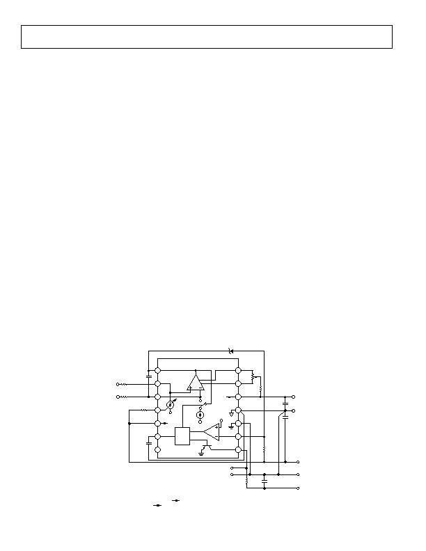
The circuit in Figure 20 accepts a true floating differential input
signal. The common-mode input, V
CM
, can be in the range
+15 V to 5 V with respect to analog ground. The signal input,
VIN, can be ? V with respect to the common-mode input. Both
inputs are low impedance; the source that drives the common-
mode input must supply the 0.5 mA drawn by the bipolar offset
current source, and the source that drives the signal input must
supply the integration current.
If less common-mode voltage range is required, then a lower
voltage Zener can be used. For example, if a 5 V Zener is used,
the VCM input can be in the range +10 V to 5 V. If the Zener is
not used at all, the common-mode range is ? V with respect to
analog ground. If no Zener is used, the 10 k?pulldown resistor
is not needed and the integrator output (Pin 1) is connected
directly to the comparator input (Pin 9).
AUTOZERO CIRCUIT
In order to exploit the full dynamic range of the AD650 VFC,
very small input voltages need to be converted. For example, a
six decade dynamic range based on a full scale of 10 V requires
accurate measurement of signals down to 10 糣. In these
situations, a well-controlled input offset voltage is imperative. A
constant offset voltage does not affect dynamic range but simply
shifts all of the frequency readings by a few hertz. However, if
the offset should change, it is not possible to distinguish
between a small change in a small input voltage and a drift of
the offset voltage. Therefore, the usable dynamic range is less.
The circuit shown in Figure 21 provides automatic adjustment
of the op amp offset voltage. The circuit uses an AD582 sample-
and-hold amplifier to control the offset, and the input voltage to
the VFC is switched between ground and the signal to be
measured via an AD7512DI analog switch. The offset of the
AD650 is adjusted by injecting a current intoor drawing a
current out ofPin 13. Note that only one of the offset null pins
is used. During the VFC norm mode, the SHA is in the hold
mode and the hold capacitor is very large, 0.1 糉, which holds
the AD650 offset constant for a long period of time.
When the circuit is in the autozero mode, the SHA is in sample
mode and behaves like an op amp. The circuit is a variation of
the classical two amplifier servo loop, where the output of the
device under test (DUT)here the DUT is the AD650 op
ampis forced to ground by the feedback action of the control
amplifierthe SHA. Because the input of the VFC circuit is
connected to ground during the autozero mode, the input
current that can flow is determined by the offset voltage of the
AD650 op amp. Because the output of the integrator stage is
forced to ground, it is known that the voltage is not changing (it
is equal to ground potential). Therefore, if the output of the
integrator is constant, its input current must be zero, so the
offset voltage has been forced to be zero. Note that the output of
the DUT could have been forced to any convenient voltage
other than ground. All that is required is that the output voltage
be known to be constant. Note also that the effect of the bias
current at the inverting input of the AD650 op amp is also
mulled in this circuit. The 1000 pF capacitor shunting the
200 k?resistor is compensation for the two amplifier servo
loop. Two integrators in a loop require a single zero for
compensation. The 3.6 k?resistor from Pin 1 of the AD650 to
the negative supply is not part of the autozero circuit, but rather,
it is required for VFC operation at 1 MHz.
OP
AMP
COMP
IN
FREQ
OUT
OUT
ONE
SHOT
8
9
10
11
13
12
7
6
5
4
3
2
1
14
INPUT
OFFSET
TRIM
10V ZENER 1N5240
NOTES
1. V
CM
IS THE COMMON MODE INPUT +15V TO 5V WITH RESPECT TO ANALOG GROUND.
2. V
IN
IS THE SIGNAL INPUT ?V WITH RESPECT TO V
CM
.
0.6V
AD650
V
S
V
IN
V
CM
INPU
V
S
1mA
S1
20k&
250k&
0.1礔
1礔
+15V
GND
GND
FREQUENCY
OUTPUT
0kHz TO 100kHz
15V
+5V
+
+
0.1礔
+
1k&
10k&
C
OS
330pF
C
I
1000pF
1.24k&
40k&
10k&
Figure 20. Differential Input
相关PDF资料 |
PDF描述 |
|---|---|
| ABB66DHRQ-S578 | CONN EDGECARD EXTEND 132POS .050 |
| EN91L5X2 | BATTERY PK 15.0V AA SIZ ALKALINE |
| AD537KH | IC V/F CONV TO-100-10 |
| 1N4004-T | RECTIFIER 400V 1A DO-41 |
| AD652KPZ | IV V-F CONVERTER SYNC 20-PLCC |
相关代理商/技术参数 |
参数描述 |
|---|---|
| AD650ADE | 制造商:Analog Devices 功能描述: |
| AD650B | 制造商:AD 制造商全称:Analog Devices 功能描述:Voltage-to-Frequency and Frequency-to-Voltage Converter |
| AD650BD | 功能描述:IC V-F/F-V CONV 1MHZ 14-CDIP RoHS:否 类别:集成电路 (IC) >> PMIC - V/F 和 F/V 转换器 系列:- 标准包装:1 系列:- 类型:频率至电压 频率 - 最大:10kHz 全量程:- 线性:±0.3% 安装类型:表面贴装 封装/外壳:8-SOIC(0.154",3.90mm 宽) 供应商设备封装:8-SOIC 包装:Digi-Reel® 其它名称:LM2917MX-8/NOPBDKR |
| AD650J | 制造商:AD 制造商全称:Analog Devices 功能描述:Voltage-to-Frequency and Frequency-to-Voltage Converter |
| AD650JN | 功能描述:IC V-F/F-V CONVERTER 14-DIP RoHS:否 类别:集成电路 (IC) >> PMIC - V/F 和 F/V 转换器 系列:- 标准包装:1 系列:- 类型:频率至电压 频率 - 最大:10kHz 全量程:- 线性:±0.3% 安装类型:表面贴装 封装/外壳:8-SOIC(0.154",3.90mm 宽) 供应商设备封装:8-SOIC 包装:Digi-Reel® 其它名称:LM2917MX-8/NOPBDKR |
发布紧急采购,3分钟左右您将得到回复。