- 您现在的位置:买卖IC网 > PDF目录22159 > AD654JRZ-REEL (Analog Devices Inc)IC V-F CONVERTER MONO 8-SOIC TR PDF资料下载
参数资料
| 型号: | AD654JRZ-REEL |
| 厂商: | Analog Devices Inc |
| 文件页数: | 10/12页 |
| 文件大小: | 354K |
| 描述: | IC V-F CONVERTER MONO 8-SOIC TR |
| 标准包装: | 2,500 |
| 类型: | 电压至频率 |
| 频率 - 最大: | 500kHz |
| 全量程: | ±50ppm/°C |
| 线性: | ±0.2% |
| 安装类型: | 表面贴装 |
| 封装/外壳: | 8-SOIC(0.154",3.90mm 宽) |
| 供应商设备封装: | 8-SOIC |
| 包装: | 带卷 (TR) |
AD654
10
REV.
8
7
6
5
1
2
3
4
AD654
68k
1k
V
IN
(0V TO 1V)
C
T
100pF
+5V
0.1F
0.1F
R
T
= 1k
+
A
J270
J270
Q1
Q2
MINIMUM
DISTANCE
+15V
V1
68k
V2
10F
10F
+
5.9k
1%
(2)
R7
8.2
MINIMUM
DISTANCE
0.1F
10F
D
5V
V3
A3-a
A3-b
18
470pF
A3-c
A3-d
V4
A3 = 74LS86
A2
LM360
D
10F
0.1F
+15V
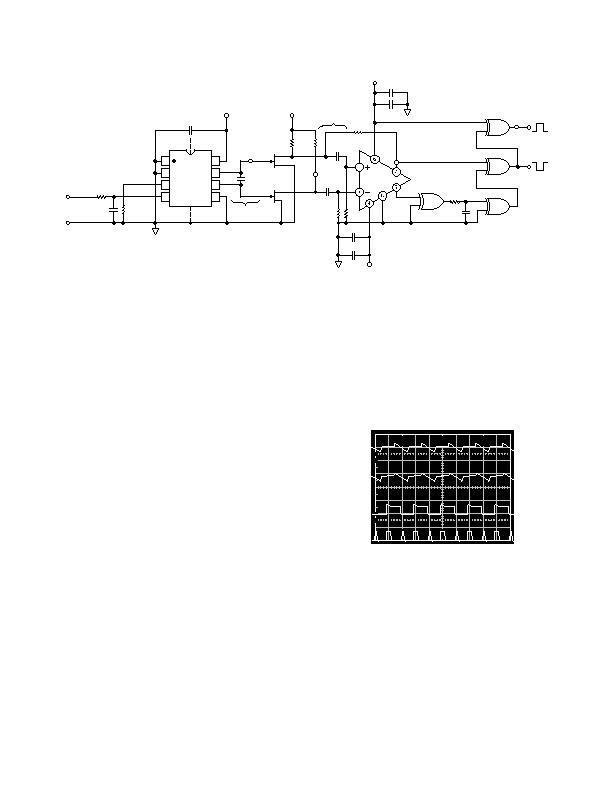
Figure 13. 2 MHz, Frequency Doubling V/F
OPERATION AT HIGHER OUTPUT FREQUENCIES
Operation of the AD654 via the conventional output (Pins 1 and
2) is speed limited to approximately 500 kHz for reasons of TTL
logic compatibility. Although the output stage may become
speed limited, the multivibrator core itself is able to oscillate to
1 MHz or more. The designer may take advantage of this feature in
order to operate the device at frequencies in excess of 500 kHz.
Figure 13 illustrates this with a circuit offering 2 MHz full scale.
In this circuit the AD654 is operated at a full scale (FS) of 1 mA,
with a C
T
of 100 pF. This achieves a basic device FS frequency
of 1 MHz across C
T
. The P channel JFETs, Q1 and Q2, buffer
the differential timing capacitor waveforms to a low impedance
level where the push-pull signal is then ac coupled to the high speed
comparator A2. Hysteresis is used, via R7, for nonambiguous
switching and to eliminate the oscillations which would other-
wise occur at low frequencies.
The net result of this is a very high speed circuit which does not
compromise the AD654 dynamic range. This is a result of the FET
buffers typically having only a few pA of bias current. The high
end dynamic range is limited, however, by parasitic package and
layout capacitances in shunt with C
T
, as well as those from each node
to ac ground. Minimizing the lead length between A26/A27 and
Q1/Q2 in PC layout will help. A ground plane will also help
stability. Figure 14 shows the waveforms V1V4 found at the
respective points shown in Figure 13.
The output of the comparator is a complementary square wave
at 1 MHz FS. Unlike pulse train output V/F converters, each
half-cycle of the AD654 output conveys information about the
input. Thus it is possible to count edges, rather than full cycles
of the output, and double the effective output frequency. The
XOR gate following A2 acts as an edge detector producing a short
pulse for each input state transition. This effectively doubles the
V/F FS frequency to 2 MHz. The final result is a 1 V full-scale
input V/F with a 2 MHz full-scale output capability; typical
nonlinearity is 0.5%.
100
90
10
0%
500ns
2V
5V
2V
5V
2V
0
2V
0
5V
0
5V
0
V1
V2
V3
V4
Figure 14. Waveforms of 2 MHz Frequency Doubler
相关PDF资料 |
PDF描述 |
|---|---|
| IDT7164S35YG | IC SRAM 64KBIT 35NS 28SOJ |
| AD7741BR | IC CONVERTER V TO FREQ 8-SOIC |
| IDT7164S35TPG | IC SRAM 64KBIT 35NS 28DIP |
| AD7741YR-REEL7 | IC CONVERTER V TO FREQ 8-SOIC |
| IDT7164S20YI8 | IC SRAM 64KBIT 20NS 28SOJ |
相关代理商/技术参数 |
参数描述 |
|---|---|
| AD654JRZ-REEL7 | 功能描述:IC V-F CONVERTER MONO 8-SOIC TR RoHS:是 类别:集成电路 (IC) >> PMIC - V/F 和 F/V 转换器 系列:- 标准包装:1 系列:- 类型:频率至电压 频率 - 最大:10kHz 全量程:- 线性:±0.3% 安装类型:表面贴装 封装/外壳:8-SOIC(0.154",3.90mm 宽) 供应商设备封装:8-SOIC 包装:Digi-Reel® 其它名称:LM2917MX-8/NOPBDKR |
| AD6555XBC | 制造商:Analog Devices 功能描述:QUAD-BAND GSM/EDGE X-PA POWER AMPLIFIER - Trays |
| AD660 | 制造商:AD 制造商全称:Analog Devices 功能描述:Monolithic 16-Bit Serial/Byte DACPORT |
| AD660_08 | 制造商:AD 制造商全称:Analog Devices 功能描述:Monolithic 16-Bit Serial/Byte DACPORT |
| AD6600 | 制造商:AD 制造商全称:Analog Devices 功能描述:Dual Channel, Gain-Ranging ADC with RSSI |
发布紧急采购,3分钟左右您将得到回复。