- 您现在的位置:买卖IC网 > PDF目录10068 > AD6600ASTZ-REEL (Analog Devices Inc)IC ADC DUAL W/RSSI 44-LQFP T/R PDF资料下载
参数资料
| 型号: | AD6600ASTZ-REEL |
| 厂商: | Analog Devices Inc |
| 文件页数: | 11/24页 |
| 文件大小: | 0K |
| 描述: | IC ADC DUAL W/RSSI 44-LQFP T/R |
| 标准包装: | 1,500 |
| 位数: | 11 |
| 采样率(每秒): | 20M |
| 数据接口: | 并联 |
| 转换器数目: | 1 |
| 功率耗散(最大): | 976mW |
| 电压电源: | 单电源 |
| 工作温度: | -40°C ~ 85°C |
| 安装类型: | 表面贴装 |
| 封装/外壳: | 44-LQFP |
| 供应商设备封装: | 44-LQFP(10x10) |
| 包装: | 带卷 (TR) |
| 输入数目和类型: | 2 个差分,双极 |
REV. 0
AD6600
–19–
315
FROM
GAIN STAGE
AVCC
GND
CLAMP
ENCODE
FLT
RESONANT
FILTER PORT
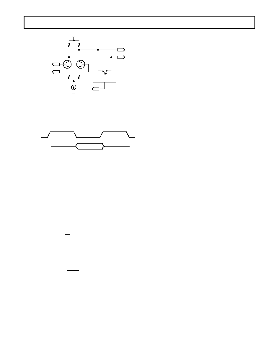
Figure 23. 4
×/8 × Amplifier Clamp Circuitry
Figure 24 shows why settling is important for this circuit. If the
4
×/8× amp does not settle (come out of clamp), the amplitude
presented to the ADC will be decreased. This results in decreased
gain when the filter capacitance is too high.
ENCODE
RESONANT
FILTER
HOLD
TRACK
HOLD
CLAMPED
SETTLING
Figure 24. 4
×/8 × Amplifier Settling
This explains why the total capacitance allowed for the external
filter varies depending on the clock rate (actually encode clock
high time). If the encode is 13 MSPS and the duty cycle is 50%,
the allowable settling time is 38.5 ns (1/2 of the encode time).
Our assumption is that the amp should be allowed to settle to
1/4 LSB in this time period. This has been proven with both
simulation and empirical analysis. If the settling is assumed to
be an RC circuit, then:
T = RC; t = time; n = number of bits
VA
e
AA
A
e
t
T
ln
T
t
ln
O
tT
nt T
n
tT
n
tT
n
=
()
=
()
=
=
=
()
1
21
1
2
1
2
1
2
/
C
T
Rl n
ns
ln
pF
TOTAL
ENCODE
=
×
()
×
()
=
×
()
=
05
8192
38 5
315
8192
13 6
.
In this case, CTOTAL includes all parasitics and external capaci-
tance. R is nominally 315
. The 8192 is (4 × 2048), which is
1/4 LSB of the converter (11 bits, 2048).
So for settling purposes, with 13 MSPS encode and 50% duty
cycle, the maximum allowable capacitance for proper settling is
CTOTAL = 13.6 pF.
As stated above, this CTOTAL includes the external capacitors,
the board parasitics, and the AD6600 parasitics. The parasitics
of the AD6600 (lead, internal bond pad and internal connec-
tions) at FLT and
FLT are 1.75 pF
±0.35 pF (differential).
If the resistors are at maximum value (315 + 20%), the maxi-
mum allowable capacitance is CTOTAL = 11.3 pF. If the duty
cycle is less than 50%, the maximum allowable capacitance is
further decreased to allow for settling.
Power Supplies
Care should be taken when selecting a power source. Linear
supplies are strongly recommended. Switching supplies tend to
have radiated components that may be “received” by the AD6600.
Each of the power supply pins should be decoupled as closely to
the package as possible using 0.1
F chip capacitors.
The AD6600 has separate digital and analog power supply pins.
The analog supplies are denoted AVCC and the digital supply
pins are denoted DVCC. Although analog and digital supplies
may be tied together, best performance is achieved when the
supplies are separate. This is because the fast digital output
swings can couple switching current back into the analog sup-
plies. Note that AVCC must be held within 5% of 5 Volts; how-
ever, the DVCC supply may be varied according to output
digital logic family. The AD6600 is specified for DVCC = 3.3 V
as this is a common supply for digital ASICS.
Output Loading
Care must be taken when designing the data receivers for the
AD6600. Note from the equivalent circuits shown earlier (see
Equivalent Circuits) that D[10:0] and RSSI[2:0] contain a
500
output series resistor. To minimize capacitive loading,
there should only be one gate on each output pin. Extra capaci-
tive loading will increase output timing and invalidate timing
specifications. CLK2
× and AB_OUT do not contain the output
series resistors. Testing for digital output timing is performed
with 10 pF loads.
Layout Information
The schematic of the evaluation board (Figure 25) represents a
typical implementation of the AD6600. A multilayer board is
recommended to achieve best results. It is highly recommended
that high quality, ceramic chip capacitors be used to decouple
each supply pin to ground directly at the device. The pinout of
the AD6600 facilitates ease of use in the implementation of high
frequency, high resolution design practices. All of the digital
outputs are segregated to two sides of the chip, with the inputs
on the opposite side for isolation purposes.
Care should be taken when routing the digital output traces. To
prevent coupling through the digital outputs into the analog
portion of the AD6600, minimal capacitive loading should be
placed on these outputs. It is recommended that a fanout of
only one be used for all AD6600 digital outputs.
The layout of the analog inputs and the external resonant filter
are critical. No digital traces must be routed near, under, or
above these portions of the circuit. The transformers used for
coupling into the analog inputs must be located as close as
possible to the analog inputs of the AD6600. The external reso-
nant filter components must be physically close to the filter-
input pins, yet separated from the analog inputs.
相关PDF资料 |
PDF描述 |
|---|---|
| IDT72V241L15JI8 | IC FIFO SYNC 4KX9 15NS 32PLCC |
| MS3102R36-79PZ | CONN RCPT 20POS BOX MNT W/PINS |
| MS27508E20A39S | CONN RCPT 39POS BOX MNT W/SCKT |
| IDT72V241L10J8 | IC FIFO SYNC 4KX9 10NS 32PLCC |
| VE-B0J-MY | CONVERTER MOD DC/DC 36V 50W |
相关代理商/技术参数 |
参数描述 |
|---|---|
| AD6600PCB | 制造商:AD 制造商全称:Analog Devices 功能描述:Dual Channel, Gain-Ranging ADC with RSSI |
| AD-6600S | 制造商:BOTHHAND 制造商全称:Bothhand USA, LP. 功能描述:ADSL TRANSFORMER |
| AD6600ST | 制造商:AD 制造商全称:Analog Devices 功能描述:Dual Channel, Gain-Ranging ADC with RSSI |
| AD6600ST/PCB | 制造商:Analog Devices 功能描述:Evaluation Board For Dual Channel, Gain-Ranging ADC With RSSI 制造商:Analog Devices 功能描述:DUAL CH, GAIN-RANGING ADC W/ RSSI - Bulk |
| AD660AN | 功能描述:IC DAC 16BIT MONO W/VREF 24-DIP RoHS:否 类别:集成电路 (IC) >> 数据采集 - 数模转换器 系列:DACPORT® 产品培训模块:Data Converter Fundamentals DAC Architectures 标准包装:750 系列:- 设置时间:7µs 位数:16 数据接口:并联 转换器数目:1 电压电源:双 ± 功率耗散(最大):100mW 工作温度:0°C ~ 70°C 安装类型:表面贴装 封装/外壳:28-LCC(J 形引线) 供应商设备封装:28-PLCC(11.51x11.51) 包装:带卷 (TR) 输出数目和类型:1 电压,单极;1 电压,双极 采样率(每秒):143k |
发布紧急采购,3分钟左右您将得到回复。