- 您现在的位置:买卖IC网 > PDF目录373890 > AD6600PCB (Analog Devices, Inc.) Dual Channel, Gain-Ranging ADC with RSSI PDF资料下载
参数资料
| 型号: | AD6600PCB |
| 厂商: | Analog Devices, Inc. |
| 英文描述: | Dual Channel, Gain-Ranging ADC with RSSI |
| 中文描述: | 双通道,增益测距型ADC的RSSI |
| 文件页数: | 17/24页 |
| 文件大小: | 303K |
| 代理商: | AD6600PCB |
REV. 0
AD6600
–17–
Table II. Selecting AD6600 Operating Mode
Output vs. Encode Clock
n
n+1
Mode
A_SEL
B_SEL
n+2
n+3
Dual: A/B
Single: A
Single: B
Not Valid
1
1
0
0
1
0
1
0
A
A
B
–
B
A
B
–
A
A
B
–
B
A
B
–
A_SEL and B_SEL are not logic inputs and should be tied
directly to ground or analog VCC (5 V analog).
In dual channel mode, the AB_OUT signal indicates which
input is currently available on the digital output. When the
AB_OUT is 1, the digital output is the digitized version of
Channel A. Likewise, when AB_OUT is 0, the Channel B is
available on the digital output (Table III).
Table III. AB_OUT for Dual Channel Operation
Output Data vs. Encode Clock
n
n+1
A_SEL and B_SEL = 1
n+2
n+3
D[10:0], RSSI[2:0]
AB_OUT
A
1
B
0
A
1
B
0
Data Output Stage
The output stage provides data in the form of mantissa, D[10:0],
and exponent, RSSI[2:0], where D[10:0] represents the output
of the 11-bit ADC coded as two
’
s complement, and RSSI[2:0]
represents the gain-range setting coded in offset binary. Table
IV shows the nominal gain-ranges for a nominal 2 V p-p differ-
ential full-scale input. Keep in mind that the actual full-scale
input voltage and power will vary with input frequency.
Table IV. Interpreting the RSSI Bits
Differential
Analog Input Voltage
(V p-p)
RSSI [2:0]
Decimal
Equiv.
Attenuation
or Gain (dB)
Binary
0.5 < V
IN
0.25 < V
IN
< 0.5
0.125 < V
IN
< 0.25
0.0625 < V
IN
< 0.125
0.03125 < V
IN
< 0.0625
V
IN
< 0.03125
101
100
011
010
001
000
5
4
3
2
1
0
–
12
–
6
0
+6
+12
+18
The digital processing chip which follows the AD6600 can com-
bine the 11 bits of two
’
s complement data with the 3 RSSI bits
to form a 16-bit equivalent output word. Table V explains how
the RSSI data can be interpreted when using a PLD or ASIC.
Basically, the circuit performs right shifts of the data depending
on the RSSI word. This can also be performed in software using
the following pseudo code fragment:
r0 = dm (rssi);
r2 = 5;
r0 = r2
–
r0;
r1 = dm (adc); (11 bits, MSB justified into DSP word)
rshift r1, r0; (arithmetic shift to extend the sign bit)
The result of the shifted data is a 16-bit fixed-point word that
can be used as any normal 16-bit word.
Table V. 16-Bit, Fixed-Point Data Format
16-Bit Data
Format
DATA
×
32
DATA
×
16
DATA
×
8
DATA
×
4
DATA
×
2
DATA
×
1
Corresponds to a
Shift Right of
RSSI
11-Bit Word
101
100
011
010
001
000
DATA
DATA
DATA
DATA
DATA
DATA
5
4
3
2
1
0
When mated with the AD6620, Digital Receive Processor Chip,
the AD6600 floating point data (mantissa + exponent) is automati-
cally converted to 16-bit two
’
s complement format by the AD6620.
APPLYING THE AD6600
Encoding the AD6600
The AD6600 encode signal must be a high quality, extremely
low phase noise source to prevent degradation of performance.
Digitizing high frequency signals (IF range 70 MHz
–
250 MHz)
places a premium on encode clock phase noise. SNR perfor-
mance can easily degrade by 3 dB
–
4 dB with 70 MHz input
signals when using a high-jitter clock source. At higher IFs (up
to 250 MHz), and with high-jitter clock sources, the higher
slew rates of the input signals reduce performance even further.
See AN-501,
Aperture Uncertainty and ADC System Performance
for complete details.
For optimum performance, the AD6600 must be clocked differ-
entially. The encode signal is usually ac-coupled into the ENC
and
ENC
pins via a transformer or capacitors. These pins are
biased internally and require no additional bias.
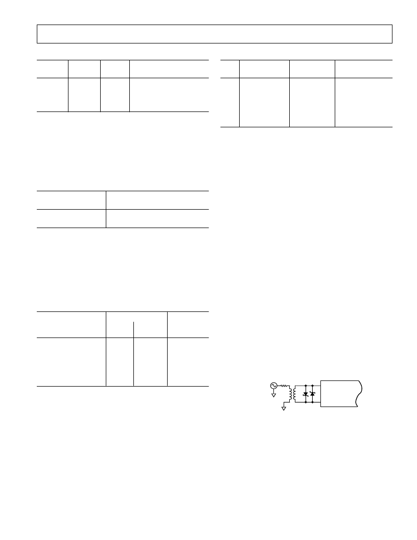
Figure 18 shows one preferred method for clocking the AD6600.
The sine source (low jitter) is converted from single-ended to
differential using an RF transformer. The back-to-back Schottky
diodes across the transformer secondary limit clock excursions
into the AD6600 to approximately 0.8 V p-p differential. This
helps prevent the larger voltage swings of the clock from feeding
through to other portions of the AD6600, and limits the noise
presented to the encode inputs. A crystal clock oscillator can
also be used to drive the RF transformer if an appropriate
limiting resistor (typically 100
) is placed in the series with
the primary.
ENCODE
ENCODE
AD6600
T1
–
1T
5DIODES
–
2810
SOSINE
100
Figure 18. Transformer-Coupled Sine Source
相关PDF资料 |
PDF描述 |
|---|---|
| AD6600ST | Dual Channel, Gain-Ranging ADC with RSSI |
| AD660AN | Monolithic 16-Bit Serial/Byte DACPORT |
| AD660AR | Monolithic 16-Bit Serial/Byte DACPORT |
| AD660BN | Monolithic 16-Bit Serial/Byte DACPORT |
| AD660BR | Monolithic 16-Bit Serial/Byte DACPORT |
相关代理商/技术参数 |
参数描述 |
|---|---|
| AD-6600S | 制造商:BOTHHAND 制造商全称:Bothhand USA, LP. 功能描述:ADSL TRANSFORMER |
| AD6600ST | 制造商:AD 制造商全称:Analog Devices 功能描述:Dual Channel, Gain-Ranging ADC with RSSI |
| AD6600ST/PCB | 制造商:Analog Devices 功能描述:Evaluation Board For Dual Channel, Gain-Ranging ADC With RSSI 制造商:Analog Devices 功能描述:DUAL CH, GAIN-RANGING ADC W/ RSSI - Bulk |
| AD660AN | 功能描述:IC DAC 16BIT MONO W/VREF 24-DIP RoHS:否 类别:集成电路 (IC) >> 数据采集 - 数模转换器 系列:DACPORT® 产品培训模块:Data Converter Fundamentals DAC Architectures 标准包装:750 系列:- 设置时间:7µs 位数:16 数据接口:并联 转换器数目:1 电压电源:双 ± 功率耗散(最大):100mW 工作温度:0°C ~ 70°C 安装类型:表面贴装 封装/外壳:28-LCC(J 形引线) 供应商设备封装:28-PLCC(11.51x11.51) 包装:带卷 (TR) 输出数目和类型:1 电压,单极;1 电压,双极 采样率(每秒):143k |
| AD660ANZ | 功能描述:IC DAC 16BIT MONO W/VREF 24-DIP RoHS:是 类别:集成电路 (IC) >> 数据采集 - 数模转换器 系列:DACPORT® 标准包装:1 系列:- 设置时间:4.5µs 位数:12 数据接口:串行,SPI? 转换器数目:1 电压电源:单电源 功率耗散(最大):- 工作温度:-40°C ~ 125°C 安装类型:表面贴装 封装/外壳:8-SOIC(0.154",3.90mm 宽) 供应商设备封装:8-SOICN 包装:剪切带 (CT) 输出数目和类型:1 电压,单极;1 电压,双极 采样率(每秒):* 其它名称:MCP4921T-E/SNCTMCP4921T-E/SNRCTMCP4921T-E/SNRCT-ND |
发布紧急采购,3分钟左右您将得到回复。