- 您现在的位置:买卖IC网 > PDF目录373890 > AD660BR (ANALOG DEVICES INC) Monolithic 16-Bit Serial/Byte DACPORT PDF资料下载
参数资料
| 型号: | AD660BR |
| 厂商: | ANALOG DEVICES INC |
| 元件分类: | DAC |
| 英文描述: | Monolithic 16-Bit Serial/Byte DACPORT |
| 中文描述: | SERIAL, PARALLEL, 8 BITS INPUT LOADING, 2.5 us SETTLING TIME, 16-BIT DAC, PDSO24 |
| 封装: | SOIC-24 |
| 文件页数: | 1/12页 |
| 文件大小: | 426K |
| 代理商: | AD660BR |
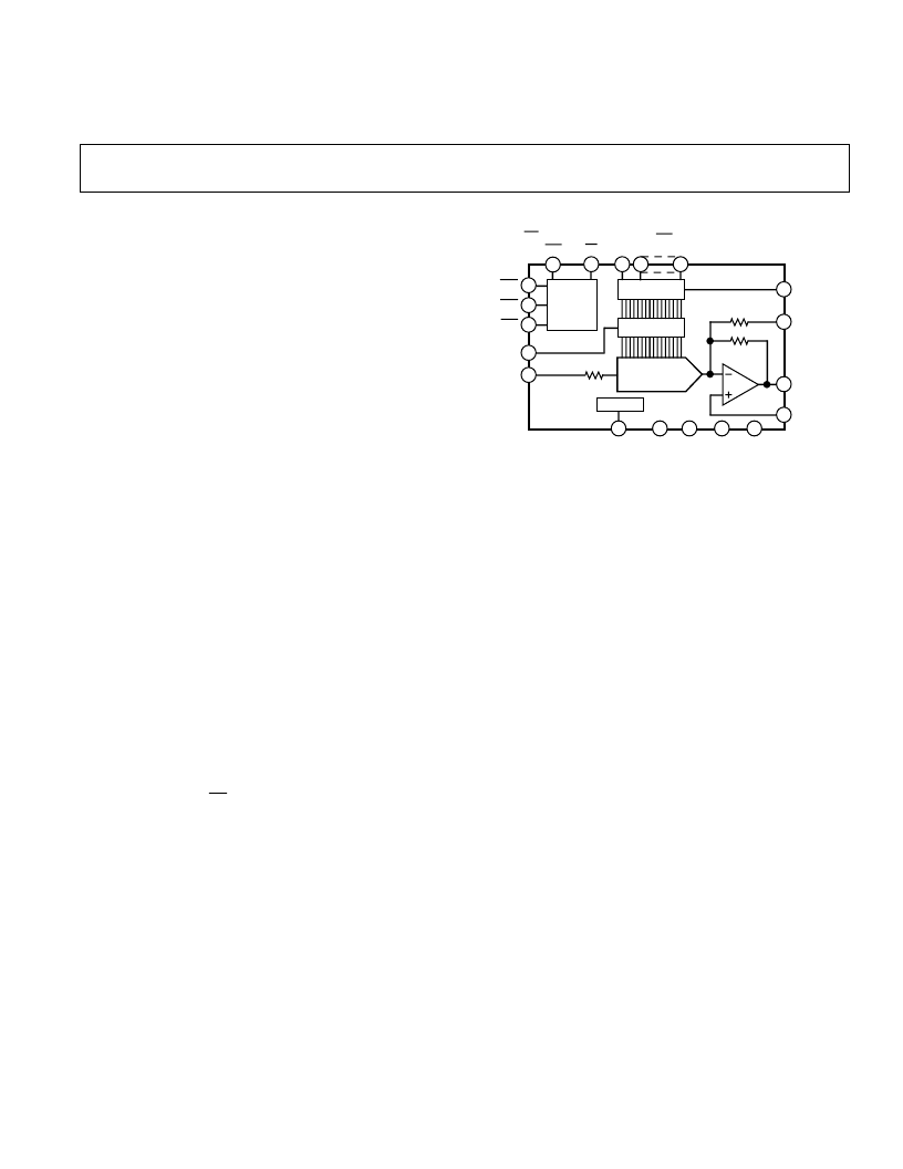
FUNCTIONAL BLOCK DIAGRAM
16-BIT LATCH
16-BIT DAC
CONTROL
LOGIC
+10V REF
16-BIT LATCH
20
24
22
21
5
11
12
16
15
14
13
17
18
19
23
AD660
10k
10.05k
10k
SIN/
DB0
DB7
S
OUT
SPAN/
BIP
OFFSET
V
OUT
AGND
REF OUT
REF IN
LDAC
SER
DGND
–V
EE
+V
CC
+V
LL
1
2
3
4
LBE
CS
HBE
CLR
MSB/LSB/
DB1
UNI/BIP CLR/
REV. A
Information furnished by Analog Devices is believed to be accurate and
reliable. However, no responsibility is assumed by Analog Devices for its
use, nor for any infringements of patents or other rights of third parties
which may result from its use. No license is granted by implication or
otherwise under any patent or patent rights of Analog Devices.
a
Monolithic 16-Bit
Serial/Byte DACPORT
AD660
FEATURES
Complete 16-Bit D/A Function
On-Chip Output Amplifier
On-Chip Buried Zener Voltage Reference
6
1 LSB Integral Linearity
15-Bit Monotonic over Temperature
Microprocessor Compatible
Serial or Byte Input
Double Buffered Latches
Fast (40 ns) Write Pulse
Asynchronous Clear (to 0 V) Function
Serial Output Pin Facilitates Daisy Chaining
Unipolar or Bipolar Output
Low Glitch: 15 nV-s
Low THD+N: 0.009%
One Technology Way, P.O. Box 9106, Norwood, MA 02062-9106, U.S.A.
Tel: 617/329-4700
Fax: 617/326-8703
PRODUCT DESCRIPTION
The AD660 DACPORT
is a complete 16-bit monolithic D/A
converter with an on-board voltage reference, double buffered
latches and output amplifier. It is manufactured on Analog De-
vices’ BiMOS II process. This process allows the fabrication of
low power CMOS logic functions on the same chip as high pre-
cision bipolar linear circuitry.
The AD660’s architecture ensures 15-bit monotonicity over
time and temperature. Integral and differential nonlinearity is
maintained at
±
0.003% max. The on-chip output amplifier pro-
vides a voltage output settling time of 10
μ
s to within 1/2 LSB
for a full-scale step.
The AD660 has an extremely flexible digital interface. Data can
be loaded into the AD660 in serial mode or as two 8-bit bytes.
This is made possible by two digital input pins which have dual
functions. The serial mode input format is pin selectable to be
MSB or LSB first. The serial output pin allows the user to daisy
chain several AD660s by shifting the data through the input
latch into the next DAC thus minimizing the number of control
lines required to SIN,
CS
and LDAC. The byte mode input for-
mat is also flexible in that the high byte or low byte data can be
loaded first. The double buffered latch structure eliminates data
skew errors and provides for simultaneous updating of DACs in
a multi-DAC system.
The AD660 is available in five grades. AN and BN versions are
specified from –40
°
C to +85
°
C and are packaged in a 24-pin
300 mil plastic DIP. AR and BR versions are also specified from
–40
°
C to +85
°
C and are packaged in a 24-pin SOIC. The SQ
version is packaged in a 24-pin 300 mil cerdip package and is
also available compliant to MIL-STD-883. Refer to the AD660/
883B data sheet for specifications and test conditions.
DACPORT is a registered trademark of Analog Devices, Inc.
PRODUCT HIGHLIGHTS
1. The AD660 is a complete 16-bit DAC, with a voltage refer-
ence, double buffered latches and output amplifier on a sin-
gle chip.
2. The internal buried Zener reference is laser trimmed to
10.000 volts with a
±
0.1% maximum error and a tempera-
ture drift performance of
±
15 ppm/
°
C. The reference is
available for external applications.
3. The output range of the AD660 is pin programmable and can
be set to provide a unipolar output range of 0 V to +10 V or
a bipolar output range of –10 V to +10 V. No external com-
ponents are required.
4. The AD660 is both dc and ac specified. DC specifications
include
±
1 LSB INL and
±
1 LSB DNL errors. AC specifi-
cations include 0.009% THD+N and 83 dB SNR.
5. The double buffered latches on the AD660 eliminate data
skew errors and allow simultaneous updating of DACs in
multi-DAC applications.
6. The CLEAR function can asynchronously set the output to
0 V regardless of whether the DAC is in unipolar or bipolar
mode.
7. The output amplifier settles within 10
μ
s to
±
1/2 LSB for a
full-scale step and within 2.5
μ
s for a 1 LSB step over tem-
perature. The output glitch is typically 15 nV-s when a full-
scale step is loaded.
相关PDF资料 |
PDF描述 |
|---|---|
| AD660SQ | Monolithic 16-Bit Serial/Byte DACPORT |
| AD660 | Monolithic 16-Bit Serial/Byte DACPORT(16位单片D/A转换器) |
| AD6620PCB | 65 MSPS Digital Receive Signal Processor |
| AD6620AS | 65 MSPS Digital Receive Signal Processor |
| AD6620S | 65 MSPS Digital Receive Signal Processor |
相关代理商/技术参数 |
参数描述 |
|---|---|
| AD660BR-REEL | 功能描述:IC DAC 16BIT MONO W/VREF 24-SOIC RoHS:否 类别:集成电路 (IC) >> 数据采集 - 数模转换器 系列:DACPORT® 产品培训模块:Lead (SnPb) Finish for COTS Obsolescence Mitigation Program 标准包装:1,000 系列:- 设置时间:1µs 位数:8 数据接口:串行 转换器数目:8 电压电源:双 ± 功率耗散(最大):941mW 工作温度:0°C ~ 70°C 安装类型:表面贴装 封装/外壳:24-SOIC(0.295",7.50mm 宽) 供应商设备封装:24-SOIC W 包装:带卷 (TR) 输出数目和类型:8 电压,单极 采样率(每秒):* |
| AD660BRZ | 功能描述:IC DAC 16BIT MONO W/VREF 24-SOIC RoHS:是 类别:集成电路 (IC) >> 数据采集 - 数模转换器 系列:DACPORT® 标准包装:1 系列:- 设置时间:4.5µs 位数:12 数据接口:串行,SPI? 转换器数目:1 电压电源:单电源 功率耗散(最大):- 工作温度:-40°C ~ 125°C 安装类型:表面贴装 封装/外壳:8-SOIC(0.154",3.90mm 宽) 供应商设备封装:8-SOICN 包装:剪切带 (CT) 输出数目和类型:1 电压,单极;1 电压,双极 采样率(每秒):* 其它名称:MCP4921T-E/SNCTMCP4921T-E/SNRCTMCP4921T-E/SNRCT-ND |
| AD660BRZ1 | 制造商:AD 制造商全称:Analog Devices 功能描述:Monolithic 16-Bit Serial/Byte DACPORT |
| AD660BRZ-REEL | 功能描述:IC DAC 16BIT MONO W/VREF 24-SOIC RoHS:是 类别:集成电路 (IC) >> 数据采集 - 数模转换器 系列:DACPORT® 产品培训模块:Data Converter Fundamentals DAC Architectures 标准包装:750 系列:- 设置时间:7µs 位数:16 数据接口:并联 转换器数目:1 电压电源:双 ± 功率耗散(最大):100mW 工作温度:0°C ~ 70°C 安装类型:表面贴装 封装/外壳:28-LCC(J 形引线) 供应商设备封装:28-PLCC(11.51x11.51) 包装:带卷 (TR) 输出数目和类型:1 电压,单极;1 电压,双极 采样率(每秒):143k |
| AD660BRZ-REEL1 | 制造商:AD 制造商全称:Analog Devices 功能描述:Monolithic 16-Bit Serial/Byte DACPORT |
发布紧急采购,3分钟左右您将得到回复。