- 您现在的位置:买卖IC网 > PDF目录373890 > AD660AR (ANALOG DEVICES INC) Monolithic 16-Bit Serial/Byte DACPORT PDF资料下载
参数资料
| 型号: | AD660AR |
| 厂商: | ANALOG DEVICES INC |
| 元件分类: | DAC |
| 英文描述: | Monolithic 16-Bit Serial/Byte DACPORT |
| 中文描述: | SERIAL, PARALLEL, 8 BITS INPUT LOADING, 2.5 us SETTLING TIME, 16-BIT DAC, PDSO24 |
| 封装: | SOIC-24 |
| 文件页数: | 11/12页 |
| 文件大小: | 426K |
| 代理商: | AD660AR |
The address decoder analyzes the input-output address pro-
duced by the processor to select the function to be performed by
the AD660, qualified by the coincidence of the Input-Output
Request (IORQ*) and Write (WR*) pins. The least significant
address bit (A0) determines if the low or high byte register of
the AD660 is active. More significant address bits select be-
tween input register loading, DAC output update, and unipolar
or bipolar clear.
A typical Z-80 software routine begins by writing the low byte of
the desired 16-bit DAC data to address 0, followed by the high
byte to address 1. The DAC output is then updated by activat-
ing LDAC with a write to address 2 (or 3). A clear to unipolar
zero occurs on a write to address 4, and a clear to bipolar zero is
performed by a write to address 5. The actual data written to
addresses 2 through 5 is irrelevant. The decoder can easily be
expanded to control as many AD660s as required.
CLR
CS
AD660
ADDRESS
DECODE
LDAC
Y0
Y2
Y1
E2
E1
A1–A15
IORQ
WR
Z80
A0-A15
A0
HBE
LBE DGND
SER
V
LL
+5V
DB0-DB7
D0-D7
Figure 11. Connections for 8-Bit Bus Interface
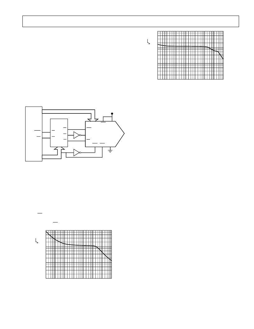
NOISE
In high resolution systems, noise is often the limiting factor. A
16-bit DAC with a 10 volt span has an LSB size of 153
μ
V
(–96 dB). Therefore, the noise floor must remain below this
level in the frequency range of interest. The AD660’s noise
spectral density is shown in Figures 12 and 13. Figure 12 shows
the DAC output noise voltage spectral density for a 20 V span
excluding the reference. This figure shows the 1/f corner
frequency at 100 Hz and the wideband noise to be below
120 nV/
√
Hz
. Figure 13 shows the reference noise voltage spec-
tral density. This figure shows the reference wideband noise to
be below 125 nV/
√
Hz
.
1000
1
1
1M
100
10
10
100k
10k
1k
100
10M
FREQUENCY – Hz
N
Figure 12. DAC Output Noise Voltage Spectral Density
1000
1
1
1M
100
10
10
100k
10k
1k
100
10M
FREQUENCY – Hz
N
Figure 13. Reference Noise Voltage Spectral Density
BOARD LAYOUT
Designing with high resolution data converters requires careful
attention to board layout. Trace impedance is the first issue. A
306
μ
A current through a 0.5
trace will develop a voltage
drop of 153
μ
V, which is 1 LSB at the 16-bit level for a 10 V
full-scale span. In addition to ground drops, inductive and
capacitive coupling need to be considered, especially when high
accuracy analog signals share the same board with digital sig-
nals. Finally, power supplies need to be decoupled in order to
filter out ac noise.
Analog and digital signals should not share a common path.
Each signal should have an appropriate analog or digital return
routed close to it. Using this approach, signal loops enclose a
small area, minimizing the inductive coupling of noise. Wide PC
tracks, large gauge wire, and ground planes are highly recom-
mended to provide low impedance signal paths. Separate analog
and digital ground planes should also be used, with a single in-
terconnection point to minimize ground loops. Analog signals
should be routed as far as possible from digital signals and
should cross them at right angles.
One feature that the AD660 incorporates to help the user layout
is that the analog pins (V
CC
, V
EE
, REF OUT, REF IN, SPAN/
BIP OFFSET, V
OUT
and AGND) are adjacent to help isolate
analog signals from digital signals.
SUPPLY DECOUPLING
The AD660 power supplies should be well filtered, well regu-
lated, and free from high frequency noise. Switching power sup-
plies are not recommended due to their tendency to generate
spikes which can induce noise in the analog system.
Decoupling capacitors should be used in very close layout prox-
imity between all power supply pins and ground. A 10
μ
F tanta-
lum capacitor in parallel with a 0.1
μ
F ceramic capacitor
provides adequate decoupling. V
CC
and V
EE
should be bypassed
to analog ground, while V
LL
should be decoupled to digital
ground.
An effort should be made to minimize the trace length between
the capacitor leads and the respective converter power supply
and common pins. The circuit layout should attempt to locate
the AD660, associated analog circuitry and interconnections as
far as possible from logic circuitry. A solid analog ground plane
around the AD660 will isolate large switching ground currents.
For these reasons, the use of wire wrap circuit construction
is not recommended; careful printed circuit construction is
preferred.
Applications Information–AD660
–11–
REV. A
相关PDF资料 |
PDF描述 |
|---|---|
| AD660BN | Monolithic 16-Bit Serial/Byte DACPORT |
| AD660BR | Monolithic 16-Bit Serial/Byte DACPORT |
| AD660SQ | Monolithic 16-Bit Serial/Byte DACPORT |
| AD660 | Monolithic 16-Bit Serial/Byte DACPORT(16位单片D/A转换器) |
| AD6620PCB | 65 MSPS Digital Receive Signal Processor |
相关代理商/技术参数 |
参数描述 |
|---|---|
| AD660AR-REEL | 制造商:Analog Devices 功能描述:DAC 1-CH R-2R/Current Steering 16-bit 24-Pin SOIC W T/R 制造商:Analog Devices 功能描述:IC, MONO 16-BIT D/A CONV - Tape and Reel |
| AD660ARZ | 功能描述:IC DAC 16BIT MONO W/VREF 24-SOIC RoHS:是 类别:集成电路 (IC) >> 数据采集 - 数模转换器 系列:DACPORT® 产品培训模块:Lead (SnPb) Finish for COTS Obsolescence Mitigation Program 标准包装:50 系列:- 设置时间:4µs 位数:12 数据接口:串行 转换器数目:2 电压电源:单电源 功率耗散(最大):- 工作温度:-40°C ~ 85°C 安装类型:表面贴装 封装/外壳:8-TSSOP,8-MSOP(0.118",3.00mm 宽) 供应商设备封装:8-uMAX 包装:管件 输出数目和类型:2 电压,单极 采样率(每秒):* 产品目录页面:1398 (CN2011-ZH PDF) |
| AD660ARZ1 | 制造商:AD 制造商全称:Analog Devices 功能描述:Monolithic 16-Bit Serial/Byte DACPORT |
| AD660ARZ-REEL | 功能描述:IC DAC 16BIT MONO W/VREF 24-SOIC RoHS:是 类别:集成电路 (IC) >> 数据采集 - 数模转换器 系列:DACPORT® 产品培训模块:Data Converter Fundamentals DAC Architectures 标准包装:750 系列:- 设置时间:7µs 位数:16 数据接口:并联 转换器数目:1 电压电源:双 ± 功率耗散(最大):100mW 工作温度:0°C ~ 70°C 安装类型:表面贴装 封装/外壳:28-LCC(J 形引线) 供应商设备封装:28-PLCC(11.51x11.51) 包装:带卷 (TR) 输出数目和类型:1 电压,单极;1 电压,双极 采样率(每秒):143k |
| AD660ARZ-REEL1 | 制造商:AD 制造商全称:Analog Devices 功能描述:Monolithic 16-Bit Serial/Byte DACPORT |
发布紧急采购,3分钟左右您将得到回复。