- 您现在的位置:买卖IC网 > PDF目录8582 > AD667KPZ-REEL (Analog Devices Inc)IC DAC 12BIT W/BUFF LATCH 28PLCC PDF资料下载
参数资料
| 型号: | AD667KPZ-REEL |
| 厂商: | Analog Devices Inc |
| 文件页数: | 4/8页 |
| 文件大小: | 0K |
| 描述: | IC DAC 12BIT W/BUFF LATCH 28PLCC |
| 标准包装: | 750 |
| 设置时间: | 3µs |
| 位数: | 12 |
| 转换器数目: | 1 |
| 电压电源: | 双 ± |
| 功率耗散(最大): | 1W |
| 工作温度: | 0°C ~ 70°C |
| 安装类型: | 表面贴装 |
| 封装/外壳: | 28-LCC(J 形引线) |
| 供应商设备封装: | 28-PLCC(11.51x11.51) |
| 包装: | 带卷 (TR) |
| 输出数目和类型: | 1 电压,单极;1 电压,双极 |
| 采样率(每秒): | * |
AD667
REV. A
–4–
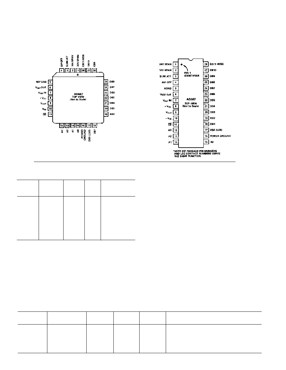
PIN CONNECTIONS
ORDERING GUIDE
Linearity
Gain
Temperature
Error Max TC Max
Model
l
Range— C
@ +25 C
ppm/ C Package Option
2
AD667JN
0 to +70
±1/2 LSB
30
Plastic DIP (N-28)
AD667JP
0 to +70
±1/2 LSB
30
PLCC (P-28A)
AD667KN
0 to +70
±1/4 LSB
15
Plastic DIP (N-28)
AD667KP
0 to +70
±1/4 LSB
15
PLCC (P-28A)
AD667AD
25 to +85
±1/2 LSB
30
Ceramic DIP (D-28)
AD667BD
–25 to +85
±1/4 LSB
15
Ceramic DIP (D-28)
AD667SD
–55 to +125
±1/2 LSB
30
Ceramic DIP (D-28)
AD667SE
–55 to +125
±1/2 LSB
30
LCC (E-28A)
AD667/883B –55 to +125
*
NOTES
*Refer to AD667/883B military data sheet.
1For details on grade and package offerings screened in accordance with MIL-STD-
883, refer to the Analog Devices Military Products Databook or current AD667/
883B data sheet.
2D = Ceramic DIP; E = Leadless Ceramic Chip Carrier; N = Plastic DIP;
P = Plastic Leaded Chip.
THE AD667 OFFERS TRUE 12-BIT PERFORMANCE
OVER THE FULL TEMPERATURE RANGE
LINEARITY ERROR: Analog Devices defines linearity error as
the maximum deviation of the actual, adjusted DAC output
from the ideal analog output (a straight line drawn from 0 to FS
– 1 LSB) for any bit combination. The AD667 is laser trimmed
to 1/4 LSB (0.006% of FS) maximum error at +25
°C for the K
and B versions and 1/2 LSB for the J, A and S versions.
MONOTONICITY: A DAC is said to be monotonic if the
output either increases or remains constant for increasing digital
inputs such that the output will always be a nondecreasing func-
tion of input. All versions of the AD667 are monotonic over
their full operating temperature range.
DIFFERENTIAL NONLINEARITY: Monotonic behavior re-
quires that the differential linearity error be less than 1 LSB
both at +25
°C and over the temperature range of interest. Dif-
ferential nonlinearity is the measure of the variation in analog
value, normalized to full scale, associated with a 1 LSB change
in digital input code. For example, for a 10 volt full-scale out-
put, a change of 1 LSB in digital input code should result in a
2.44 mV change in the analog output (1 LSB = 10 V
× 1/4096 =
2.44 mV). If in actual use, however, a 1 LSB change in the
input code results in a change of only 0.61 mV (1/4 LSB) in
analog output, the differential linearity error would be –1.83 mV,
or –3/4 LSB. The AD667K and B grades have a max differential
linearity error of 1/2 LSB, which specifies that every step will be
at least 1/2 LSB and at most 1 1/2 LSB.
Table I. Output Voltage Range Connections
Output
Digital
Connect
Range
Input Codes
Pin 9 to
Pin 1 to
Pin 2 to
Pin 4 to
±10 V
Offset Binary
1
9
NC
6 (Through 50
Fixed or 100 Trim Resistor)
±5 V
Offset Binary
1 and 2
2 and 9
1 and 9
6 (Through 50
Fixed or 100 Trim Resistor)
±2.5 V
Offset Binary
2
3
9
6 (Through 50
Fixed or 100 Trim Resistor)
0 V to +10 V
Straight Binary
1 and 2
2 and 9
1 and 9
5 (or Optional Trim—See Figure 2)
0 V to +5 V
Straight Binary
2
3
9
5 (or Optional Trim—See Figure 2)
PLCC, LCC
DIP
相关PDF资料 |
PDF描述 |
|---|---|
| VE-B6B-MW-B1 | CONVERTER MOD DC/DC 95V 100W |
| LTC1597-1BIG | IC D/A CONV 16BIT PAR 28-SSOP |
| LTC1597-1BIG#TRPBF | IC D/A CONV 16BIT PAR 28-SSOP |
| LTC2755BCUP-16#TRPBF | IC DAC 16BIT CUR OUT 64-QFN |
| AD7840KNZ | IC DAC 14BIT LC2MOS VOUT 24-DIP |
相关代理商/技术参数 |
参数描述 |
|---|---|
| AD667SD | 功能描述:数模转换器- DAC IC - 12-BIT D/A CONVERTER RoHS:否 制造商:Texas Instruments 转换器数量:1 DAC 输出端数量:1 转换速率:2 MSPs 分辨率:16 bit 接口类型:QSPI, SPI, Serial (3-Wire, Microwire) 稳定时间:1 us 最大工作温度:+ 85 C 安装风格:SMD/SMT 封装 / 箱体:SOIC-14 封装:Tube |
| AD667SD/883B | 功能描述:数模转换器- DAC IC - 12-BIT D/A CONVERTER RoHS:否 制造商:Texas Instruments 转换器数量:1 DAC 输出端数量:1 转换速率:2 MSPs 分辨率:16 bit 接口类型:QSPI, SPI, Serial (3-Wire, Microwire) 稳定时间:1 us 最大工作温度:+ 85 C 安装风格:SMD/SMT 封装 / 箱体:SOIC-14 封装:Tube |
| AD667SD883B | 制造商:AD 功能描述:New |
| AD667SD883BQ | 制造商:AD 功能描述:* |
| AD667SE | 功能描述:数模转换器- DAC MPU-Compatible IC 12-BIT RoHS:否 制造商:Analog Devices 转换器数量:4 DAC 输出端数量:4 转换速率: 分辨率:12 bit 接口类型:Serial (I2C) 稳定时间: 最大工作温度:+ 105 C 安装风格: 封装 / 箱体:TSSOP 封装:Reel |
发布紧急采购,3分钟左右您将得到回复。