- 您现在的位置:买卖IC网 > PDF目录8582 > AD667KPZ-REEL (Analog Devices Inc)IC DAC 12BIT W/BUFF LATCH 28PLCC PDF资料下载
参数资料
| 型号: | AD667KPZ-REEL |
| 厂商: | Analog Devices Inc |
| 文件页数: | 6/8页 |
| 文件大小: | 0K |
| 描述: | IC DAC 12BIT W/BUFF LATCH 28PLCC |
| 标准包装: | 750 |
| 设置时间: | 3µs |
| 位数: | 12 |
| 转换器数目: | 1 |
| 电压电源: | 双 ± |
| 功率耗散(最大): | 1W |
| 工作温度: | 0°C ~ 70°C |
| 安装类型: | 表面贴装 |
| 封装/外壳: | 28-LCC(J 形引线) |
| 供应商设备封装: | 28-PLCC(11.51x11.51) |
| 包装: | 带卷 (TR) |
| 输出数目和类型: | 1 电压,单极;1 电压,双极 |
| 采样率(每秒): | * |
AD667
REV. A
–6–
Small resistors may be added to the feedback resistors in order
to accomplish small modifications in the scaling. For example, if
a 10.24 V full scale is desired, a 140
1% low TC metal-film
resistor can be added in series with the internal (nominal) 5k
feedback resistor, and the gain trim potentiometer (between
Pins 6 and 7) should be increased to 200
. In the bipolar
mode, increase the value of the bipolar offset trim potentiometer
also to 200
.
GROUNDING RULES
The AD667 brings out separate analog and power grounds to
allow optimum connections for low noise and high speed perfor-
mance. These grounds should be tied together at one point,
usually the device power ground. The separate ground returns
are provided to minimize current flow in low level signal paths.
The analog ground at Pin 5 is the ground point for the output
amplifier and is thus the “high quality” ground for the AD667;
it should be connected directly to the analog reference point of
the system. The power ground at Pin 16 can be connected to
the most convenient ground point; analog power return is
preferred. If power ground contains high frequency noise be-
yond 200 mV, this noise may feed through the converter, thus
some caution will be required in applying these grounds.
It is also important to apply decoupling capacitors properly on
the power supplies for the AD667 and the output amplifier. The
correct method for decoupling is to connect a capacitor from
each power supply pin of the AD667 to the analog ground pin
of the AD667. Any load driven by the output amplifier should
also be referred to the analog ground pin.
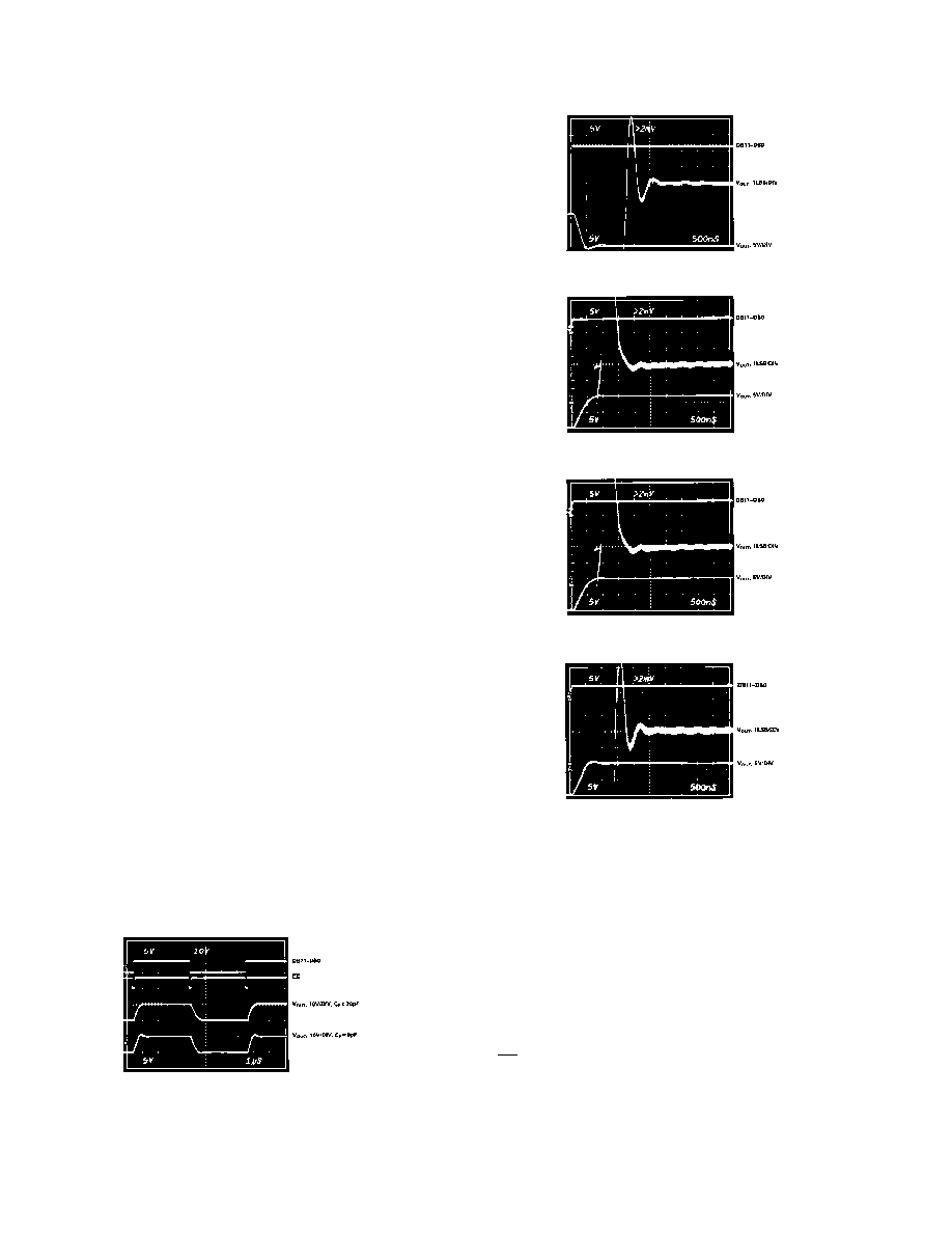
OPTIMIZING SETTLING TIME
The dynamic performance of the AD667’s output amplifier can
be optimized by adding a small (20 pF) capacitor across the
feedback resistor. Figure 4 shows the improvement in both
large-signal and small-signal settling for the 10 V range. In Fig-
ure 4a, the top trace shows the data inputs (DB11–DB0 tied to-
gether), the second trace shows the CS pulse (A3–A0 tied low),
and the lower two traces show the analog outputs for CF = 0 pF
and 20 pF respectively.
Figures 4b and 4c show the settling time for the transition from
all bits on to all bits off. Note that the settling time to
±1/2 LSB
for the 10 V step is improved from 2.4 microseconds to 1.6 mi-
croseconds by the addition of the 20 pF capacitor.
Figures 4d and 4e show the settling time for the transition from
all bits off to all bits on. The improvement in settling time
gained by adding CC = 20 pF is similar.
a. Large Scale Settling
b. Fine-Scale Settling, CF = 0 pF
c. Fine-Scale Settling, CF = 20 pF
d. Fine-Scale Settling, CF = 0 pF
e. Fine-Scale Settling, CF = 20 pF
Figure 4. Settling Time Performance
DIGITAL CIRCUIT DETAILS
The bus interface logic of the AD667 consists of four indepen-
dently addressable registers in two ranks. The first rank consists
of three four-bit registers which can be loaded directly from a
4-, 8-, 12-, or 16-bit microprocessor bus. Once the complete
12-bit data word has been assembled in the first rank, it can be
loaded into the 12-bit register of the second rank. This
double-buffered organization avoids the generation of spurious
analog output values. Figure 5 shows the block diagram of the
AD667 logic section.
The latches are controlled by the address inputs, A0–A3, and
the CS input. All control inputs are active low, consistent with
general practice in microprocessor systems. The four address
lines each enable one of the four latches, as indicated in Table II.
All latches in the AD667 are level-triggered. This means that
data present during the time when the control signals are valid
will enter the latch. When any one of the control signals returns
high, the data is latched.
相关PDF资料 |
PDF描述 |
|---|---|
| VE-B6B-MW-B1 | CONVERTER MOD DC/DC 95V 100W |
| LTC1597-1BIG | IC D/A CONV 16BIT PAR 28-SSOP |
| LTC1597-1BIG#TRPBF | IC D/A CONV 16BIT PAR 28-SSOP |
| LTC2755BCUP-16#TRPBF | IC DAC 16BIT CUR OUT 64-QFN |
| AD7840KNZ | IC DAC 14BIT LC2MOS VOUT 24-DIP |
相关代理商/技术参数 |
参数描述 |
|---|---|
| AD667SD | 功能描述:数模转换器- DAC IC - 12-BIT D/A CONVERTER RoHS:否 制造商:Texas Instruments 转换器数量:1 DAC 输出端数量:1 转换速率:2 MSPs 分辨率:16 bit 接口类型:QSPI, SPI, Serial (3-Wire, Microwire) 稳定时间:1 us 最大工作温度:+ 85 C 安装风格:SMD/SMT 封装 / 箱体:SOIC-14 封装:Tube |
| AD667SD/883B | 功能描述:数模转换器- DAC IC - 12-BIT D/A CONVERTER RoHS:否 制造商:Texas Instruments 转换器数量:1 DAC 输出端数量:1 转换速率:2 MSPs 分辨率:16 bit 接口类型:QSPI, SPI, Serial (3-Wire, Microwire) 稳定时间:1 us 最大工作温度:+ 85 C 安装风格:SMD/SMT 封装 / 箱体:SOIC-14 封装:Tube |
| AD667SD883B | 制造商:AD 功能描述:New |
| AD667SD883BQ | 制造商:AD 功能描述:* |
| AD667SE | 功能描述:数模转换器- DAC MPU-Compatible IC 12-BIT RoHS:否 制造商:Analog Devices 转换器数量:4 DAC 输出端数量:4 转换速率: 分辨率:12 bit 接口类型:Serial (I2C) 稳定时间: 最大工作温度:+ 105 C 安装风格: 封装 / 箱体:TSSOP 封装:Reel |
发布紧急采购,3分钟左右您将得到回复。