参数资料
| 型号: | AD669BR-REEL |
| 厂商: | Analog Devices Inc |
| 文件页数: | 11/12页 |
| 文件大小: | 0K |
| 描述: | IC DAC 16BIT MONO VREF 28-SOIC |
| 产品培训模块: | Data Converter Fundamentals DAC Architectures |
| 产品变化通告: | AD669 Improvement Change 11/Jul/2012 |
| 标准包装: | 1,000 |
| 系列: | DACPORT® |
| 设置时间: | 10µs |
| 位数: | 16 |
| 数据接口: | 并联 |
| 转换器数目: | 1 |
| 电压电源: | 双 ± |
| 功率耗散(最大): | 625mW |
| 工作温度: | -40°C ~ 85°C |
| 安装类型: | 表面贴装 |
| 封装/外壳: | 28-SOIC(0.295",7.50mm 宽) |
| 供应商设备封装: | 28-SOIC W |
| 包装: | 带卷 (TR) |
| 输出数目和类型: | 1 电压,单极;1 电压,双极 |
| 采样率(每秒): | 167k |
AD669
REV. A
–8–
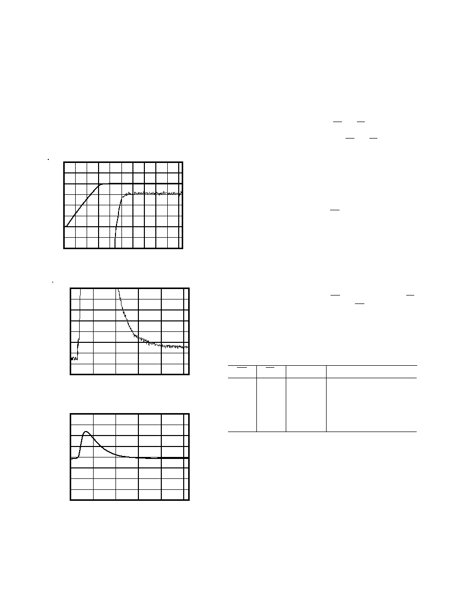
OUTPUT SETTLING AND GLITCH
The AD669’s output buffer amplifier typically settles to within
0.0008% FS (l/2 LSB) of its final value in 8
s for a full-scale
step. Figures 7a and 7b show settling for a full-scale and an LSB
step, respectively, with a 2 k
, 1000 pF load applied. The guar-
anteed maximum settling time at +25
°C for a full-scale step is
13
s with this load. The typical settling time for a 1 LSB step is
2.5
s.
The digital-to-analog glitch impulse is specified as 15 nV-s typi-
cal. Figure 7c shows the typical glitch impulse characteristic at
the code 011 . . . 111 to 100 . . . 000 transition when loading
the second rank register from the first rank register.
20
–10
0
+10
10
600
400
200
0
–200
–400
–600
VOLTS
s
V
a. –10 V to +10 V Full-Scale Step Settling
5
0
600
400
200
–200
–400
–600
s
V
1
23
4
b. LSB Step Settling
5
0
+10
–10
s
mV
1
23
4
c. D-to-A Glitch Impulse
Figure 7. Output Characteristics
DIGITAL CIRCUIT DETAILS
The bus interface logic of the AD669 consists of two indepen-
dently addressable registers in two ranks. The first rank consists
of a 16-bit register which is loaded directly from a 16-bit micro-
processor bus. Once the 16-bit data word has been loaded in the
first rank, it can be loaded into the 16-bit register of the second
rank. This double-buffered organization avoids the generation of
spurious analog output values.
The first rank latch is controlled by CS and L1. Both of these
inputs are active low and are level-triggered. This means that
data present during the time when both CS and L1 are low will
enter the latch. When either one of these signals returns high,
the data is latched.
The second rank latch is controlled by LDAC. This input is ac-
tive high and is also level-triggered. Data that is present when
LDAC is high will enter the latch, and hence the DAC will
change state. When this pin returns low, the data is latched in
the DAC.
Note that LDAC is not gated with CS or any other control sig-
nal. This makes it possible to simultaneously update all of the
AD669’s present in a multi-DAC system by tying the LDAC
pins together. After the first rank register of each DAC has been
individually loaded and latched, the second rank registers are
then brought high together, updating all of the DACs at the
same time. To reduce bit skew, it is suggested to leave 100 ns
between the first rank load and the second rank load.
The first rank latch and second rank latch can be used together
in a master-slave or edge-triggered configuration. This mode of
operation occurs when LDAC and CS are tied together with L1
tied to ground. Rising edges on the LDAC-CS pair will update
the DAC with the data presented preceding the edge. The tim-
ing diagram for operation in this mode can be seen in Figure lb.
Note, however, that the sum of tLOW and tHIGH must be long
enough to allow the DAC output to settle to its new value.
Table I. AD669 Truth Table
CS
L1
LDAC
Operation
0
X
First Rank Enable
X
1
X
First Rank Latched
1
X
First Rank Latched
X
1
Second Rank Enabled
X
0
Second Rank Latched
0
1
All Latches Transparent
“X” = Don’t Care
It is possible to make the second rank register transparent by ty-
ing Pin 23 high. Any data appearing in the first rank register will
then appear at the output of the DAC. It should be noted, how-
ever, that the deskewing provided by the second rank latch is
then defeated, and glitch impulse may increase. If it is desired to
make both registers transparent, this can be done by tying Pins
5 and 6 low and Pin 23 high. Table I shows the truth table for
the AD669, while the timing diagram is found in Figure 1.
INPUT CODING
The AD669 uses positive-true binary input coding. Logic “1” is
represented by an input voltage greater than 2.0 V, and Logic
“0” is defined as an input voltage less than 0.8 V.
相关PDF资料 |
PDF描述 |
|---|---|
| DAC8413FPC-REEL | IC DAC 12BIT QUAD V-OUT 28-PLCC |
| AD9735BBCZ | IC DAC 12BIT 1.2GSPS 160-CSPBGA |
| AD7225LPZ | IC DAC 8BIT QUAD W/AMP 28-PLCC |
| AD9776BSVZ | IC DAC 12BIT DUAL 1GSPS 100TQFP |
| ADDAC80D-CBI-V | IC DAC 12BIT LOW COST 24-CDIP |
相关代理商/技术参数 |
参数描述 |
|---|---|
| AD669BRZ | 功能描述:IC DAC 16BIT MONO W/VREF 28-SOIC RoHS:是 类别:集成电路 (IC) >> 数据采集 - 数模转换器 系列:DACPORT® 产品培训模块:Lead (SnPb) Finish for COTS Obsolescence Mitigation Program 标准包装:50 系列:- 设置时间:4µs 位数:12 数据接口:串行 转换器数目:2 电压电源:单电源 功率耗散(最大):- 工作温度:-40°C ~ 85°C 安装类型:表面贴装 封装/外壳:8-TSSOP,8-MSOP(0.118",3.00mm 宽) 供应商设备封装:8-uMAX 包装:管件 输出数目和类型:2 电压,单极 采样率(每秒):* 产品目录页面:1398 (CN2011-ZH PDF) |
| AD669BRZ-REEL | 功能描述:IC DAC 16BIT MONO VREF 28-SOIC RoHS:是 类别:集成电路 (IC) >> 数据采集 - 数模转换器 系列:DACPORT® 产品培训模块:Data Converter Fundamentals DAC Architectures 标准包装:750 系列:- 设置时间:7µs 位数:16 数据接口:并联 转换器数目:1 电压电源:双 ± 功率耗散(最大):100mW 工作温度:0°C ~ 70°C 安装类型:表面贴装 封装/外壳:28-LCC(J 形引线) 供应商设备封装:28-PLCC(11.51x11.51) 包装:带卷 (TR) 输出数目和类型:1 电压,单极;1 电压,双极 采样率(每秒):143k |
| AD669SQ | 功能描述:数模转换器- DAC IC MONO 16-BIT RoHS:否 制造商:Analog Devices 转换器数量:4 DAC 输出端数量:4 转换速率: 分辨率:12 bit 接口类型:Serial (I2C) 稳定时间: 最大工作温度:+ 105 C 安装风格: 封装 / 箱体:TSSOP 封装:Reel |
| AD669SQ/883B | 功能描述:数模转换器- DAC IC MONO 16-BIT RoHS:否 制造商:Analog Devices 转换器数量:4 DAC 输出端数量:4 转换速率: 分辨率:12 bit 接口类型:Serial (I2C) 稳定时间: 最大工作温度:+ 105 C 安装风格: 封装 / 箱体:TSSOP 封装:Reel |
| AD66BS | 制造商:POP 功能描述: 制造商:RIVETS 功能描述: |
发布紧急采购,3分钟左右您将得到回复。