参数资料
| 型号: | AD669BR-REEL |
| 厂商: | Analog Devices Inc |
| 文件页数: | 12/12页 |
| 文件大小: | 0K |
| 描述: | IC DAC 16BIT MONO VREF 28-SOIC |
| 产品培训模块: | Data Converter Fundamentals DAC Architectures |
| 产品变化通告: | AD669 Improvement Change 11/Jul/2012 |
| 标准包装: | 1,000 |
| 系列: | DACPORT® |
| 设置时间: | 10µs |
| 位数: | 16 |
| 数据接口: | 并联 |
| 转换器数目: | 1 |
| 电压电源: | 双 ± |
| 功率耗散(最大): | 625mW |
| 工作温度: | -40°C ~ 85°C |
| 安装类型: | 表面贴装 |
| 封装/外壳: | 28-SOIC(0.295",7.50mm 宽) |
| 供应商设备封装: | 28-SOIC W |
| 包装: | 带卷 (TR) |
| 输出数目和类型: | 1 电压,单极;1 电压,双极 |
| 采样率(每秒): | 167k |
AD669
REV. A
–9–
Unipolar coding is straight binary, where all zeros (0000H) on
the data inputs yields a zero analog output and all ones
(FFFFH) yields an analog output 1 LSB below full scale.
Bipolar coding is offset binary, where an input code of 0000H
yields a minus full-scale output, an input of FFFFH yields an
output 1 LSB below positive full scale, and zero occurs for an
input code with only the MSB on (8000H).
The AD669 can be used with twos complement input coding if
an inverter is used on the MSB (DB15).
DIGITAL INPUT CONSIDERATIONS
The threshold of the digital input circuitry is set at 1.4 volts.
The input lines can thus interface with any type of 5 volt logic.
The AD669 data and control inputs will float to indeterminate
logic states if left open. It is important that CS and L1 be con-
nected to DGND and Chat LDAC be tied to VLL if these pins
are not used.
Fanout for the AD669 is 40 when used with a standard low
power Schottky gate output device.
16-BIT MICROPROCESSOR INTERFACE
The 16-bit parallel registers of the AD669 allow direct interfac-
ing to 16-bit general purpose and DSP microprocessor buses.
The following examples illustrate typical AD669 interface
configurations.
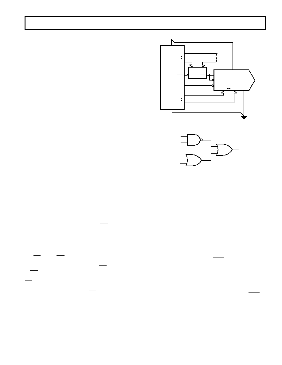
AD669 TO ADSP-2101 INTERFACE
The flexible interface of the AD669 minimizes the required
“glue” logic when it is connected in configurations such as the
one shown in Figure 8. The AD669 is mapped into the ADSP-
2101’s memory space and requires two wait states using a 12.5
MHz processor clock.
In this configuration, the ADSP-2101 is set up to use the inter-
nal timer to interrupt the processor at the desired sample rate.
The WR pin and data lines D8–D23 from the ADSP-2101 are
tied directly to the L1 and DB0 through DB15 pins of the
AD669, respectively. The decoded signal CS1 is connected to
both CS and LDAC. When a timer interrupt is detected, the
ADSP-2101 automatically vectors to the appropriate service
routine with minimal overhead. The interrupt routine then in-
structs the processor to execute a data memory write to the ad-
dress of the AD669.
The WR pin and CS1 both go low causing the first 16-bit latch
inside the AD669 to be transparent. The data present in the first
rank is then latched by the rising edge of WR. The rising edge
of CS1 will cause the second rank 16-bit latch to become
transparent updating the output of the DAC. The length of
WR
is extended by two wait states to comply with the timing
requirements of tLOW shown in Figure 1b. It is important to
latch the data with the rising edge of WR rather than the decoded
CS1.
This is necessary to comply with the tDH specification of
the AD669.
A0
D8
ADSP-2101
DGND
+5V
DECODER
ADDRESS BUS
LDAC
AD669
DGND
DB0
DATA BUS
DMS
WR
CS1
CS
L1
A13
DB15
D23
V
LL
V
LL
V
OUT
a. ADSP-2101 to AD669 Interface
A13
A12
A11
DMS
CS1
b. Typical Address Decoder
Figure 8. ADSP-2101 to AD669 Interface
Figure 8b shows the circuitry a typical decoder might include.
In this case, a data memory write to any address in the range
3000H to 3400H will result in the AD669 being updated. These
decoders will vary greatly depending on the number of devices
memory-mapped by the processor.
AD669 TO DSP56001 INTERFACE
Figure 9 shows the interface between the AD669 and the
DSP56001. Like the ADSP-2101, the AD669 is mapped into
the DSP56001’s memory space. This application was tested
with a processor clock of 20.48 MHz (tCYC = 97.66 ns) although
faster rates are possible.
An external clock connected to the IRQA pin of the DSP56001
interrupts the processor at the desired sample rate. If ac perfor-
mance is important, this clock should be synchronous with the
DSP56001 processor clock. Asynchronous clocks will cause jit-
ter on the latch signal due to the uncertainty associated with the
acknowledgment of the interrupt. A synchronous clock is easily
generated by dividing down the clock from the DSP crystal. If
ac performance is not important, it is not necessary for IRQA to
be synchronous.
After the interrupt is acknowledged, the interrupt routine ini-
tiates a memory write cycle. All of the AD669 control inputs are
相关PDF资料 |
PDF描述 |
|---|---|
| DAC8413FPC-REEL | IC DAC 12BIT QUAD V-OUT 28-PLCC |
| AD9735BBCZ | IC DAC 12BIT 1.2GSPS 160-CSPBGA |
| AD7225LPZ | IC DAC 8BIT QUAD W/AMP 28-PLCC |
| AD9776BSVZ | IC DAC 12BIT DUAL 1GSPS 100TQFP |
| ADDAC80D-CBI-V | IC DAC 12BIT LOW COST 24-CDIP |
相关代理商/技术参数 |
参数描述 |
|---|---|
| AD669BRZ | 功能描述:IC DAC 16BIT MONO W/VREF 28-SOIC RoHS:是 类别:集成电路 (IC) >> 数据采集 - 数模转换器 系列:DACPORT® 产品培训模块:Lead (SnPb) Finish for COTS Obsolescence Mitigation Program 标准包装:50 系列:- 设置时间:4µs 位数:12 数据接口:串行 转换器数目:2 电压电源:单电源 功率耗散(最大):- 工作温度:-40°C ~ 85°C 安装类型:表面贴装 封装/外壳:8-TSSOP,8-MSOP(0.118",3.00mm 宽) 供应商设备封装:8-uMAX 包装:管件 输出数目和类型:2 电压,单极 采样率(每秒):* 产品目录页面:1398 (CN2011-ZH PDF) |
| AD669BRZ-REEL | 功能描述:IC DAC 16BIT MONO VREF 28-SOIC RoHS:是 类别:集成电路 (IC) >> 数据采集 - 数模转换器 系列:DACPORT® 产品培训模块:Data Converter Fundamentals DAC Architectures 标准包装:750 系列:- 设置时间:7µs 位数:16 数据接口:并联 转换器数目:1 电压电源:双 ± 功率耗散(最大):100mW 工作温度:0°C ~ 70°C 安装类型:表面贴装 封装/外壳:28-LCC(J 形引线) 供应商设备封装:28-PLCC(11.51x11.51) 包装:带卷 (TR) 输出数目和类型:1 电压,单极;1 电压,双极 采样率(每秒):143k |
| AD669SQ | 功能描述:数模转换器- DAC IC MONO 16-BIT RoHS:否 制造商:Analog Devices 转换器数量:4 DAC 输出端数量:4 转换速率: 分辨率:12 bit 接口类型:Serial (I2C) 稳定时间: 最大工作温度:+ 105 C 安装风格: 封装 / 箱体:TSSOP 封装:Reel |
| AD669SQ/883B | 功能描述:数模转换器- DAC IC MONO 16-BIT RoHS:否 制造商:Analog Devices 转换器数量:4 DAC 输出端数量:4 转换速率: 分辨率:12 bit 接口类型:Serial (I2C) 稳定时间: 最大工作温度:+ 105 C 安装风格: 封装 / 箱体:TSSOP 封装:Reel |
| AD66BS | 制造商:POP 功能描述: 制造商:RIVETS 功能描述: |
发布紧急采购,3分钟左右您将得到回复。