- 您现在的位置:买卖IC网 > PDF目录17024 > AD676-EB (Analog Devices Inc)BOARD EVAL SAMPLING ADC AD676 PDF资料下载
参数资料
| 型号: | AD676-EB |
| 厂商: | Analog Devices Inc |
| 文件页数: | 5/16页 |
| 文件大小: | 0K |
| 描述: | BOARD EVAL SAMPLING ADC AD676 |
| 标准包装: | 1 |
| ADC 的数量: | 1 |
| 位数: | 16 |
| 采样率(每秒): | 100k |
| 数据接口: | 并联 |
| 输入范围: | ±VREF |
| 在以下条件下的电源(标准): | 360mW @ 100kSPS |
| 工作温度: | 0°C ~ 70°C |
| 已用 IC / 零件: | AD676 |
| 已供物品: | 板 |
| 相关产品: | AD676JDZ-ND - IC ADC 16BIT SAMPLING 28-CDIP AD676KN-ND - IC ADC 16BIT SAMPLING 28-DIP AD676BD-ND - IC ADC 16BIT SAMPLING 28-CDIP AD676AD-ND - IC ADC 16BIT SAMPLING 28-CDIP AD676KD-ND - IC ADC 16BIT 100KSPS 28-CDIP AD676JN-ND - IC ADC 16BIT 100KSPS 28-DIP AD676JD-ND - IC ADC 16BIT SAMPLING 28-CDIP |
AD676
REV. A
–13–
AC PERFORMANCE
AC parameters, which include S/(N+D), THD, etc., reflect the
AD676’s effect on the spectral content of the analog input sig-
nal. Figures 12 through 16 provide information on the AD676’s
ac performance under a variety of conditions.
As a general rule, averaging the results from several conversions
reduces the effects of noise, and therefore improves such param-
eters as S/(N+D). AD676 performance may be optimized by
operating the device at its maximum sample rate of 100 kSPS
and digitally filtering the resulting bit stream to the desired signal
bandwidth. This succeeds in distributing noise over a wider
frequency range, thus reducing the noise density in the fre-
quency band of interest. This subject is discussed in the follow-
ing section.
OVERSAMPLING AND NOISE FILTERING
The Nyquist rate for a converter is defined as one-half its sam-
pling rate. This is established by the Nyquist theorem, which re-
quires that a signal he sampled at a rate corresponding to at
least twice its highest frequency component of interest in order
to preserve the informational content. Oversampling is a conver-
sion technique in which the sampling frequency is more than
twice the frequency bandwidth of interest. In audio applications,
the AD676 can operate at a 2
FS oversampling rate, where
FS = 48 kHz.
In quantized systems, the informational content of the analog
input is represented in the frequency spectrum from dc to the
Nyquist rate of the converter. Within this same spectrum are
higher frequency noise and signal components. Antialias, or low
pass, filters are used at the input to the ADC to reduce these
noise and signal components so that their aliased components
do not corrupt the baseband spectrum. However, wideband
noise contributed by the AD676 will not be reduced by the
antialias filter. The AD676 quantization noise is evenly distrib-
uted from dc to the Nyquist rate, and this fact can be used to
minimize its overall affect.
The AD676 quantization noise effects can be reduced by
oversampling–sampling at a rate higher than that defined by the
Nyquist theorem. This spreads the noise energy over a band-
width wider than the frequency band of interest. By judicious
selection of a digital decimation filter, noise frequencies outside
the bandwidth of interest may be eliminated.
The process of analog to digital conversion inherently produces
noise, known as quantization noise. The magnitude of this noise
is a function of the resolution of the converter, and manifests it-
self as a limit to the theoretical signal-to-noise ratio achievable.
This limit is described by S/(N+D) = (6.02n + 1.76 + 10 log
FS/2FA) dB, where n is the resolution of the converter in bits, FS
is the sampling frequency, and Fa is the signal bandwidth of in-
terest. For audio bandwidth applications, the AD676 is capable
of operating at a 2
oversample rate (96 kSPS), which typically
produces an improvement in S/(N+D) of 3 dB compared with
operating at the Nyquist conversion rate of 48 kSPS. Over-
sampling has another advantage as well; the demands on the
antialias filter are lessened. In summary, system performance is
optimized by running the AD676 at or near its maximum sam-
pling rate of 100 kHz and digitally filtering the resulting spec-
trum to eliminate undesired frequencies.
DC CODE UNCERTAINTY
Ideally, a fixed dc input should result in the same output code
for repetitive conversions. However, as a consequence of system
noise and circuit noise, for a given input voltage there is a range
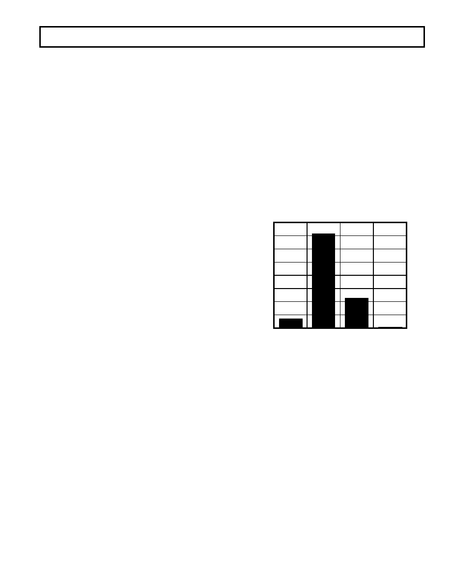
of output codes which may occur. Figure 9 is a histogram of the
codes resulting from 1000 conversions of a typical input voltage
by the AD676 used with a 10 V reference.
2
1
0
–1
DEVIATION FROM CORRECT CODE – LSBs
NUMBER
OF
CODE
HITS
800
0
200
400
600
Figure 9. Distribution of Codes from 1000 Conversions,
Relative to the Correct Code
The standard deviation of this distribution is approximately 0.5
LSBs. If less uncertainty is desired, averaging multiple conver-
sions will narrow this distribution by the inverse of the square
root of the number of samples; i.e., the average of 4 conversions
would have a standard deviation of 0.25 LSBs.
相关PDF资料 |
PDF描述 |
|---|---|
| AD9211-200EBZ | BOARD EVAL FOR AD9211-200 |
| HW-V5-ML521-UNI-G-J | EVALUATION PLATFORM VIRTEX-5 |
| HW-V4-ML423-UNI-G-J | EVALUATION PLATFORM VIRTEX-4 |
| GCM22DRPS | CONN EDGECARD 44POS DIP .156 SLD |
| AD9219-65EBZ | BOARD EVALUATION FOR AD9219 |
相关代理商/技术参数 |
参数描述 |
|---|---|
| AD676JD | 功能描述:IC ADC 16BIT SAMPLING 28-CDIP RoHS:否 类别:集成电路 (IC) >> 数据采集 - 模数转换器 系列:- 标准包装:1 系列:- 位数:14 采样率(每秒):83k 数据接口:串行,并联 转换器数目:1 功率耗散(最大):95mW 电压电源:双 ± 工作温度:0°C ~ 70°C 安装类型:通孔 封装/外壳:28-DIP(0.600",15.24mm) 供应商设备封装:28-PDIP 包装:管件 输入数目和类型:1 个单端,双极 |
| AD676JDZ | 功能描述:IC ADC 16BIT SAMPLING 28-CDIP RoHS:是 类别:集成电路 (IC) >> 数据采集 - 模数转换器 系列:- 标准包装:1 系列:- 位数:14 采样率(每秒):83k 数据接口:串行,并联 转换器数目:1 功率耗散(最大):95mW 电压电源:双 ± 工作温度:0°C ~ 70°C 安装类型:通孔 封装/外壳:28-DIP(0.600",15.24mm) 供应商设备封装:28-PDIP 包装:管件 输入数目和类型:1 个单端,双极 |
| AD676JDZ# | 制造商:Analog Devices 功能描述: |
| AD676JN | 功能描述:IC ADC 16BIT 100KSPS 28-DIP RoHS:否 类别:集成电路 (IC) >> 数据采集 - 模数转换器 系列:- 标准包装:1 系列:- 位数:14 采样率(每秒):83k 数据接口:串行,并联 转换器数目:1 功率耗散(最大):95mW 电压电源:双 ± 工作温度:0°C ~ 70°C 安装类型:通孔 封装/外壳:28-DIP(0.600",15.24mm) 供应商设备封装:28-PDIP 包装:管件 输入数目和类型:1 个单端,双极 |
| AD676JNZ | 功能描述:IC ADC 16BIT 100KSPS 28-DIP RoHS:是 类别:集成电路 (IC) >> 数据采集 - 模数转换器 系列:- 标准包装:1 系列:- 位数:14 采样率(每秒):83k 数据接口:串行,并联 转换器数目:1 功率耗散(最大):95mW 电压电源:双 ± 工作温度:0°C ~ 70°C 安装类型:通孔 封装/外壳:28-DIP(0.600",15.24mm) 供应商设备封装:28-PDIP 包装:管件 输入数目和类型:1 个单端,双极 |
发布紧急采购,3分钟左右您将得到回复。