- 您现在的位置:买卖IC网 > PDF目录17024 > AD676-EB (Analog Devices Inc)BOARD EVAL SAMPLING ADC AD676 PDF资料下载
参数资料
| 型号: | AD676-EB |
| 厂商: | Analog Devices Inc |
| 文件页数: | 6/16页 |
| 文件大小: | 0K |
| 描述: | BOARD EVAL SAMPLING ADC AD676 |
| 标准包装: | 1 |
| ADC 的数量: | 1 |
| 位数: | 16 |
| 采样率(每秒): | 100k |
| 数据接口: | 并联 |
| 输入范围: | ±VREF |
| 在以下条件下的电源(标准): | 360mW @ 100kSPS |
| 工作温度: | 0°C ~ 70°C |
| 已用 IC / 零件: | AD676 |
| 已供物品: | 板 |
| 相关产品: | AD676JDZ-ND - IC ADC 16BIT SAMPLING 28-CDIP AD676KN-ND - IC ADC 16BIT SAMPLING 28-DIP AD676BD-ND - IC ADC 16BIT SAMPLING 28-CDIP AD676AD-ND - IC ADC 16BIT SAMPLING 28-CDIP AD676KD-ND - IC ADC 16BIT 100KSPS 28-CDIP AD676JN-ND - IC ADC 16BIT 100KSPS 28-DIP AD676JD-ND - IC ADC 16BIT SAMPLING 28-CDIP |
AD676
REV. A
–14–
MICROPROCESSOR INTERFACE
The AD676 is ideally suited for use in both traditional dc mea-
surement applications supporting a microprocessor, and in ac
signal processing applications interfacing to a digital signal pro-
cessor. The AD676 is designed to interface with a 16-bit data
bus, providing all output data bits in a single read cycle. A vari-
ety of external buffers, such as 74HC541, can be used with the
AD676 to provide 3-state outputs, high driving capability, and
to prevent bus noise from coupling into the ADC. The following
sections illustrate the use of the AD676 with a representative
digital signal processor and microprocessor. These circuits pro-
vide general interface practices which are applicable to other
processor choices.
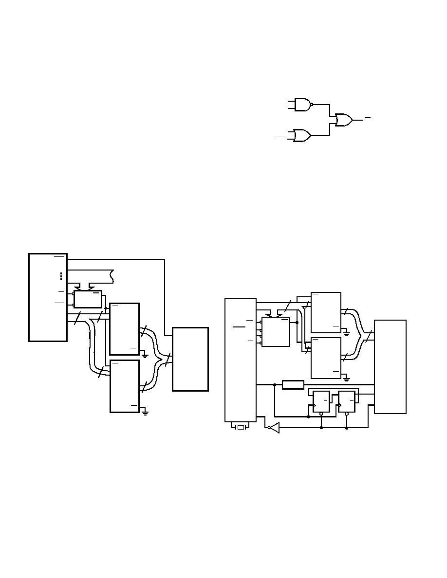
ADSP-2101
Figure 10a shows the AD676 interfaced to the ADSP-2101 DSP
processor. The AD676 buffers are mapped in the ADSP-2101’s
memory space, requiring one wait state when using a 12.5 MHz
processor clock.
The falling edge of BUSY interrupts the processor, indicating
that new data is ready. The ADSP-2101 automatically jumps to
the appropriate service routine with minimal overhead. The in-
terrupt routine then instructs the processor to read the new data
using a memory read instruction.
A0
A13
D8 – D23
ADSP-2101
IRQ2
RD
DMS
DECODER
CS
ADDRESS BUS
Y1 – Y8
A1 – A3
74HC541
G1
G2
Y1 – Y8
A1 – A3
74HC541
G1
G2
BUSY
BIT 1 – BIT 16
AD676
16
8
16
8
Figure 10a.
Figure 10b shows circuitry which would be included by a typical
address decoder for the output buffers. In this case, a data
memory access to any address in the range 3000H to 37FFH
will result in the output buffers being enabled.
The AD676 CLK and SAMPLE can be generated by dividing
down the system clock as described earlier (Figure 3), or if the
ADSP-2101 serial port clocks are not being used, they can be
programmed to generate CLK and SAMPLE.
A13
A12
A11
DMS
CS
Figure 10b.
80286
The 80286 16-bit microprocessor can be interfaced to a buff-
ered AD676 without any generation of wait states. As seen in
Figure 11, BUSY can be used both to control the AD676 clock
and to alert the processor when new data is ready. In the system
shown, the 80286 should be configured in an edge triggered, di-
rect interrupt mode (integrated controller provides the interrupt
vector). Since the 80286 does not latch interrupt signals, the in-
terrupt needs to be internally acknowledged before BUSY goes
HIGH again during the next AD676 conversion (BUSY = 0).
Depending on whether the AD676 buffers are mapped into
memory or 1/0 space, the interrupt service routine will read the
data by using either the MOV or the IN instruction. To be able
to read all the 16 bits at once, and thereby increase the 80286’s
efficiency, the buffers should be located at an even address.
AD0 – AD15
ALE
CLKOUT
INT 0
80286
RD
PCSO – 6
S2
DECODER
CS
16
Y1 – Y8
A1 – A8
74HC541
G1
G2
Y1 – Y8
A1 – A8
74HC541
G1
G2
8
DIVIDER
D
CLR
Q
D
CLR
Q
74HC04
74HC74
BIT1 – BIT16
SAMPLE
CLK
BUSY
AD676
2MHz
16
8
Figure 11.
相关PDF资料 |
PDF描述 |
|---|---|
| AD9211-200EBZ | BOARD EVAL FOR AD9211-200 |
| HW-V5-ML521-UNI-G-J | EVALUATION PLATFORM VIRTEX-5 |
| HW-V4-ML423-UNI-G-J | EVALUATION PLATFORM VIRTEX-4 |
| GCM22DRPS | CONN EDGECARD 44POS DIP .156 SLD |
| AD9219-65EBZ | BOARD EVALUATION FOR AD9219 |
相关代理商/技术参数 |
参数描述 |
|---|---|
| AD676JD | 功能描述:IC ADC 16BIT SAMPLING 28-CDIP RoHS:否 类别:集成电路 (IC) >> 数据采集 - 模数转换器 系列:- 标准包装:1 系列:- 位数:14 采样率(每秒):83k 数据接口:串行,并联 转换器数目:1 功率耗散(最大):95mW 电压电源:双 ± 工作温度:0°C ~ 70°C 安装类型:通孔 封装/外壳:28-DIP(0.600",15.24mm) 供应商设备封装:28-PDIP 包装:管件 输入数目和类型:1 个单端,双极 |
| AD676JDZ | 功能描述:IC ADC 16BIT SAMPLING 28-CDIP RoHS:是 类别:集成电路 (IC) >> 数据采集 - 模数转换器 系列:- 标准包装:1 系列:- 位数:14 采样率(每秒):83k 数据接口:串行,并联 转换器数目:1 功率耗散(最大):95mW 电压电源:双 ± 工作温度:0°C ~ 70°C 安装类型:通孔 封装/外壳:28-DIP(0.600",15.24mm) 供应商设备封装:28-PDIP 包装:管件 输入数目和类型:1 个单端,双极 |
| AD676JDZ# | 制造商:Analog Devices 功能描述: |
| AD676JN | 功能描述:IC ADC 16BIT 100KSPS 28-DIP RoHS:否 类别:集成电路 (IC) >> 数据采集 - 模数转换器 系列:- 标准包装:1 系列:- 位数:14 采样率(每秒):83k 数据接口:串行,并联 转换器数目:1 功率耗散(最大):95mW 电压电源:双 ± 工作温度:0°C ~ 70°C 安装类型:通孔 封装/外壳:28-DIP(0.600",15.24mm) 供应商设备封装:28-PDIP 包装:管件 输入数目和类型:1 个单端,双极 |
| AD676JNZ | 功能描述:IC ADC 16BIT 100KSPS 28-DIP RoHS:是 类别:集成电路 (IC) >> 数据采集 - 模数转换器 系列:- 标准包装:1 系列:- 位数:14 采样率(每秒):83k 数据接口:串行,并联 转换器数目:1 功率耗散(最大):95mW 电压电源:双 ± 工作温度:0°C ~ 70°C 安装类型:通孔 封装/外壳:28-DIP(0.600",15.24mm) 供应商设备封装:28-PDIP 包装:管件 输入数目和类型:1 个单端,双极 |
发布紧急采购,3分钟左右您将得到回复。