参数资料
| 型号: | AD676BD |
| 厂商: | Analog Devices Inc |
| 文件页数: | 16/16页 |
| 文件大小: | 0K |
| 描述: | IC ADC 16BIT SAMPLING 28-CDIP |
| 标准包装: | 1 |
| 位数: | 16 |
| 采样率(每秒): | 100k |
| 数据接口: | 并联 |
| 转换器数目: | 2 |
| 功率耗散(最大): | 480mW |
| 电压电源: | 模拟和数字,双 ± |
| 工作温度: | -40°C ~ 85°C |
| 安装类型: | 通孔 |
| 封装/外壳: | 28-CDIP(0.605",15.37mm) |
| 供应商设备封装: | 28-CDIP |
| 包装: | 管件 |
| 输入数目和类型: | 1 个单端,双极 |
| 配用: | AD676-EB-ND - BOARD EVAL SAMPLING ADC AD676 |
AD676
REV. A
–9–
CONTINUOUS CONVERSION
For maximum throughput rate, the AD676 can be operated in a
continuous convert mode (see Figure 2b). This is accomplished
by utilizing the fact that SAMPLE will no longer be ignored af-
ter BUSY goes LOW, so an acquisition may be initiated even
during the HIGH time of the 17th CLK pulse for maximum
throughput rate while enabling full settling of the sample/hold
circuitry. If SAMPLE is already HIGH when BUSY goes LOW
at the end of a conversion, then an acquisition is immediately
initiated and tS and tC start from that time. Data from the previ-
ous conversion may be latched up to tSD before BUSY goes
LOW or tOD after the rising edge of the 17th clock pulse. How-
ever, it is preferred that latching occur on or after the falling
edge of BUSY.
Care must he taken to adhere to the minimum/maximum timing
requirements in order to preserve conversion accuracy.
GENERAL CONVERSION GUIDELINES
During signal acquisition and conversion, care should be taken
with the logic inputs to avoid digital feedthrough noise. It is pos-
sible to run CLK continuously, even during the sample period.
However, CLK edges during the sampling period, and especially
when SAMPLE goes LOW, may inject noise into the sampling
process. The AD676 is tested with no CLK cycles during the
sampling period. The BUSY signal can be used to prevent the
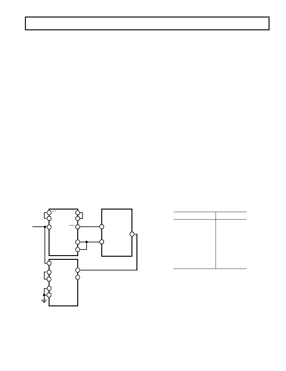
clock from running during acquisition, as illustrated in Figure 3.
In this circuit BUSY is used to reset the circuitry which divides
the system clock down to provide the AD676 CLK. This serves
to interrupt the clock until after the input signal has been ac-
quired, which has occurred when BUSY goes HIGH. When the
conversion is completed and BUSY goes LOW, the circuit in
Figure 3 truncates the 17th CLK pulse width which is tolerable
because only its rising edge is critical.
5
2
10
7
1
7
12
9
4
11
12.288MHz
SYSTEM
CLOCK
CLK
74HC175
2D
1Q
CLR
3D
2Q
3Q
1D
BUSY
CLK
AD676
9
SAMPLE
2
8
9
12
6
13
1
1QD
74HC393
1CLR
2CLR
2QD
2QC
1CLK
2CLK
Figure 3.
Figure 3 also illustrates the use of a counter (74HC393) to de-
rive the AD676 SAMPLE command from the system clock
when a continuous convert mode is desirable. Pin 9 (2QC) pro-
vides a 96 kHz sample rate for the AD676 when used with a
12.288 MHz system clock. Alternately, Pin 8 (2QD) could be
used for a 48 kHz rate.
If a continuous clock is used, then the user must avoid CLK
edges at the instant of disconnecting VIN which occurs at the
falling edge of SAMPLE (see tSC specification). The duty cycle
of CLK may vary, but both the HIGH (tCH) and LOW (tCL )
phases must conform to those shown in the timing specifica-
tions. The internal comparator makes its decisions on the rising
edge of CLK. To avoid a negative edge transition disturbing the
comparator’s settling, tCL should be at least half the value of tCLK.
To also avoid transitions disturbing the internal comparator’s
settling, it is not recommended that the SAMPLE pin change
state toward the end of a CLK cycle.
During a conversion, internal dc error terms such as comparator
voltage offset are sampled, stored on internal capacitors and
used to correct for their corresponding errors when needed. Be-
cause these voltages are stored on capacitors, they are subject to
leakage decay and so require refreshing. For this reason there is
a maximum conversion time tC (1000
s). From the time
SAMPLE goes HIGH to the completion of the 17th CLK pulse,
no more than 1000
s should elapse for specified performance.
However, there is no restriction to the maximum time between
conversions.
Output coding for the AD676 is twos complement, as shown in
Table I. By inverting the MSB, the coding can be converted to
offset binary. The AD676 is designed to limit output coding in
the event of out-of-range inputs.
Table I. Output Coding
VIN
Output Code
>Full Scale
011 . . . 11
Full Scale
011 . . . 11
Full Scale – 1 LSB
011 . . . 10
Midscale + 1 LSB
000 . . . 01
Midscale
000 . . . 00
Midscale – 1 LSB
111 . . . 11
–Full Scale + 1 LSB
100 . . . 01
–Full Scale
100 . . . 00
<–Full Scale
100 . . . 00
相关PDF资料 |
PDF描述 |
|---|---|
| AD677BD | IC ADC 16BIT SAMPLING 16-CDIP |
| AD678BJ | IC ADC 12BIT SAMPLING 44-JLCC |
| AD679BJ | IC ADC 14BIT SAMPLING 44-JLCC |
| AD7111BQ | IC DAC LOGARITHMIC 16-CDIP |
| AD7170BCPZ-REEL7 | IC ADC 12BIT SIGMA-DELTA 10LFCSP |
相关代理商/技术参数 |
参数描述 |
|---|---|
| AD676-EB | 功能描述:BOARD EVAL SAMPLING ADC AD676 RoHS:否 类别:编程器,开发系统 >> 评估板 - 模数转换器 (ADC) 系列:- 产品培训模块:Obsolescence Mitigation Program 标准包装:1 系列:- ADC 的数量:1 位数:12 采样率(每秒):94.4k 数据接口:USB 输入范围:±VREF/2 在以下条件下的电源(标准):- 工作温度:-40°C ~ 85°C 已用 IC / 零件:MAX11645 已供物品:板,软件 |
| AD676JD | 功能描述:IC ADC 16BIT SAMPLING 28-CDIP RoHS:否 类别:集成电路 (IC) >> 数据采集 - 模数转换器 系列:- 标准包装:1 系列:- 位数:14 采样率(每秒):83k 数据接口:串行,并联 转换器数目:1 功率耗散(最大):95mW 电压电源:双 ± 工作温度:0°C ~ 70°C 安装类型:通孔 封装/外壳:28-DIP(0.600",15.24mm) 供应商设备封装:28-PDIP 包装:管件 输入数目和类型:1 个单端,双极 |
| AD676JDZ | 功能描述:IC ADC 16BIT SAMPLING 28-CDIP RoHS:是 类别:集成电路 (IC) >> 数据采集 - 模数转换器 系列:- 标准包装:1 系列:- 位数:14 采样率(每秒):83k 数据接口:串行,并联 转换器数目:1 功率耗散(最大):95mW 电压电源:双 ± 工作温度:0°C ~ 70°C 安装类型:通孔 封装/外壳:28-DIP(0.600",15.24mm) 供应商设备封装:28-PDIP 包装:管件 输入数目和类型:1 个单端,双极 |
| AD676JDZ# | 制造商:Analog Devices 功能描述: |
| AD676JN | 功能描述:IC ADC 16BIT 100KSPS 28-DIP RoHS:否 类别:集成电路 (IC) >> 数据采集 - 模数转换器 系列:- 标准包装:1 系列:- 位数:14 采样率(每秒):83k 数据接口:串行,并联 转换器数目:1 功率耗散(最大):95mW 电压电源:双 ± 工作温度:0°C ~ 70°C 安装类型:通孔 封装/外壳:28-DIP(0.600",15.24mm) 供应商设备封装:28-PDIP 包装:管件 输入数目和类型:1 个单端,双极 |
发布紧急采购,3分钟左右您将得到回复。