参数资料
| 型号: | AD676BD |
| 厂商: | Analog Devices Inc |
| 文件页数: | 2/16页 |
| 文件大小: | 0K |
| 描述: | IC ADC 16BIT SAMPLING 28-CDIP |
| 标准包装: | 1 |
| 位数: | 16 |
| 采样率(每秒): | 100k |
| 数据接口: | 并联 |
| 转换器数目: | 2 |
| 功率耗散(最大): | 480mW |
| 电压电源: | 模拟和数字,双 ± |
| 工作温度: | -40°C ~ 85°C |
| 安装类型: | 通孔 |
| 封装/外壳: | 28-CDIP(0.605",15.37mm) |
| 供应商设备封装: | 28-CDIP |
| 包装: | 管件 |
| 输入数目和类型: | 1 个单端,双极 |
| 配用: | AD676-EB-ND - BOARD EVAL SAMPLING ADC AD676 |
AD676
REV. A
–10–
POWER SUPPLIES AND DECOUPLING
The AD676 has three power supply input pins. VCC and VEE
provide the supply voltages to operate the analog portions of the
AD676 including the ADC and sample-hold amplifier (SHA).
VDD provides the supply voltage which operates the digital por-
tions of the AD676 including the data output buffers and the
autocalibration controller.
As with most high performance linear circuits, changes in the
power supplies can produce undesired changes in the perfor-
mance of the circuit. Optimally, well regulated power supplies
with less than 1% ripple should be selected. The ac output im-
pedance of a power supply is a complex function of frequency,
and in general will increase with frequency. In other words, high
frequency switching such as that encountered with digital cir-
cuitry requires fast transient currents which most power supplies
cannot adequately provide. This results in voltage spikes on the
supplies. If these spikes exceed the
±5% tolerance of the ±12 V
supplies or the
±10% limits of the +5 V supply, ADC perfor-
mance will degrade. Additionally, spikes at frequencies higher
than 100 kHz will also degrade performance. To compensate for
the finite ac output impedance of the supplies, it is necessary to
store “reserves” of charge in bypass capacitors. These capacitors
can effectively lower the ac impedance presented to the AD676
power inputs which in turn will significantly reduce the magni-
tude of the voltage spikes. For bypassing to be effective, certain
guidelines should be followed. Decoupling capacitors, typically
0.1
F, should be placed as closely as possible to each power
supply pin of the AD676. It is essential that these capacitors be
placed physically close to the IC to minimize the inductance of
the PCB trace between the capacitor and the supply pin. The
logic supply (VDD) should be decoupled to digital common and
the analog supplies (Vcc and VEE) to analog common. The ref-
erence input is also considered as a power supply pin in this re-
gard and the same decoupling procedures apply. These points
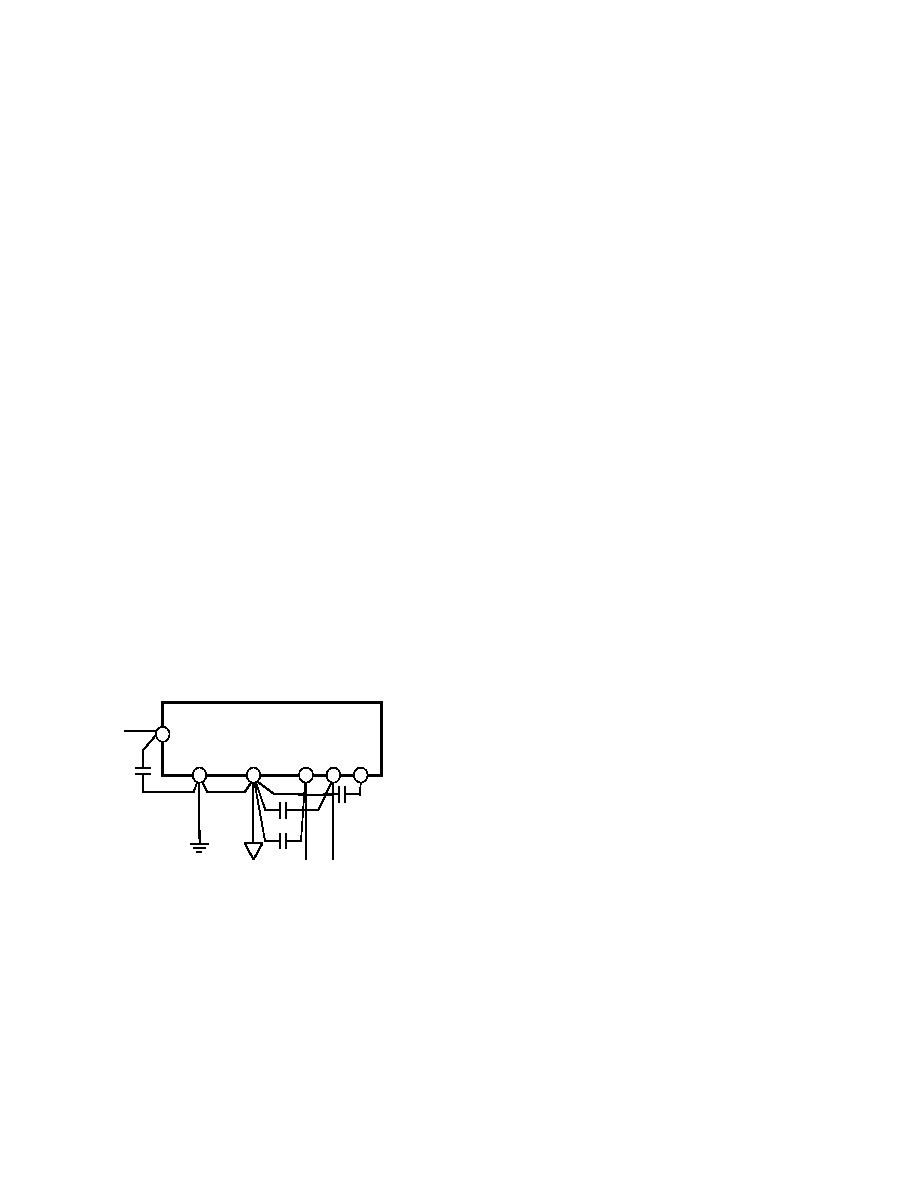
are displayed in Figure 4.
+5V
12V –12V
SYSTEM
ANALOG
COMMON
SYSTEM
DIGITAL
COMMON
AGND
DGND
AD676
17
12
13
11
18
EE
V
CC
V
11
V
REF
VDD
0.1
F
0.1
F
0.1
F
0.1
F
Figure 4. Grounding and Decoupling the AD676
Additionally, it is beneficial to have large capacitors (>47
F)
located at the point where the power connects to the PCB with
10
F capacitors located in the vicinity of the ADC to further
reduce low frequency ripple. In systems that will be subjected to
particularly harsh environmental noise, additional decoupling
may be necessary. RC-filtering on each power supply combined
with dedicated voltage regulation can substantially decrease
power supply ripple effects (this is further detailed in Figure 7).
BOARD LAYOUT
Designing with high resolution data converters requires careful
attention to board layout. Trace impedance is a significant issue.
A 1.22 mA current through a 0.5
trace will develop a voltage
drop of 0.6 mV, which is 4 LSBs at the 16-bit level for a 10 V
full-scale span. In addition to ground drops, inductive and ca-
pacitive coupling need to be considered, especially when high
accuracy analog signals share the same board with digital
signals.
Analog and digital signals should not share a common return
path. Each signal should have an appropriate analog or digital
return routed close to it. Using this approach, signal loops en-
close a small area, minimizing the inductive coupling of noise.
Wide PC tracks, large gauge wire, and ground planes are highly
recommended to provide low impedance signal paths. Separate
analog and digital ground planes are also desirable, with a single
interconnection point at the AD676 to minimize interference
between analog and digital circuitry. Analog signals should be
routed as far as possible from digital signals and should cross
them, if at all, only at right angles. A solid analog ground plane
around the AD676 will isolate it from large switching ground
currents. For these reasons, the use of wire wrap circuit con-
struction will not provide adequate performance; careful printed
circuit board construction is preferred.
GROUNDING
The AD676 has three grounding pins, designated ANALOG
GROUND (AGND), DIGITAL GROUND (DGND) and
ANALOG GROUND SENSE (AGND SENSE). The analog
ground pin is the “high quality” ground reference point for the
device, and should be connected to the analog common point in
the system.
AGND SENSE is intended to be connected to the input signal
ground reference point. This allows for slight differences in level
between the analog ground point in the system and the input
signal ground point. However no more than 100 mV is recom-
mended between the AGND and the AGND SENSE pins for
specified performance.
相关PDF资料 |
PDF描述 |
|---|---|
| AD677BD | IC ADC 16BIT SAMPLING 16-CDIP |
| AD678BJ | IC ADC 12BIT SAMPLING 44-JLCC |
| AD679BJ | IC ADC 14BIT SAMPLING 44-JLCC |
| AD7111BQ | IC DAC LOGARITHMIC 16-CDIP |
| AD7170BCPZ-REEL7 | IC ADC 12BIT SIGMA-DELTA 10LFCSP |
相关代理商/技术参数 |
参数描述 |
|---|---|
| AD676-EB | 功能描述:BOARD EVAL SAMPLING ADC AD676 RoHS:否 类别:编程器,开发系统 >> 评估板 - 模数转换器 (ADC) 系列:- 产品培训模块:Obsolescence Mitigation Program 标准包装:1 系列:- ADC 的数量:1 位数:12 采样率(每秒):94.4k 数据接口:USB 输入范围:±VREF/2 在以下条件下的电源(标准):- 工作温度:-40°C ~ 85°C 已用 IC / 零件:MAX11645 已供物品:板,软件 |
| AD676JD | 功能描述:IC ADC 16BIT SAMPLING 28-CDIP RoHS:否 类别:集成电路 (IC) >> 数据采集 - 模数转换器 系列:- 标准包装:1 系列:- 位数:14 采样率(每秒):83k 数据接口:串行,并联 转换器数目:1 功率耗散(最大):95mW 电压电源:双 ± 工作温度:0°C ~ 70°C 安装类型:通孔 封装/外壳:28-DIP(0.600",15.24mm) 供应商设备封装:28-PDIP 包装:管件 输入数目和类型:1 个单端,双极 |
| AD676JDZ | 功能描述:IC ADC 16BIT SAMPLING 28-CDIP RoHS:是 类别:集成电路 (IC) >> 数据采集 - 模数转换器 系列:- 标准包装:1 系列:- 位数:14 采样率(每秒):83k 数据接口:串行,并联 转换器数目:1 功率耗散(最大):95mW 电压电源:双 ± 工作温度:0°C ~ 70°C 安装类型:通孔 封装/外壳:28-DIP(0.600",15.24mm) 供应商设备封装:28-PDIP 包装:管件 输入数目和类型:1 个单端,双极 |
| AD676JDZ# | 制造商:Analog Devices 功能描述: |
| AD676JN | 功能描述:IC ADC 16BIT 100KSPS 28-DIP RoHS:否 类别:集成电路 (IC) >> 数据采集 - 模数转换器 系列:- 标准包装:1 系列:- 位数:14 采样率(每秒):83k 数据接口:串行,并联 转换器数目:1 功率耗散(最大):95mW 电压电源:双 ± 工作温度:0°C ~ 70°C 安装类型:通孔 封装/外壳:28-DIP(0.600",15.24mm) 供应商设备封装:28-PDIP 包装:管件 输入数目和类型:1 个单端,双极 |
发布紧急采购,3分钟左右您将得到回复。