- 您现在的位置:买卖IC网 > PDF目录10031 > AD678AJ (Analog Devices Inc)IC ADC 12BIT 200KSPS 44-JLCC PDF资料下载
参数资料
| 型号: | AD678AJ |
| 厂商: | Analog Devices Inc |
| 文件页数: | 2/14页 |
| 文件大小: | 0K |
| 描述: | IC ADC 12BIT 200KSPS 44-JLCC |
| 标准包装: | 1 |
| 位数: | 12 |
| 采样率(每秒): | 200k |
| 数据接口: | 并联 |
| 转换器数目: | 2 |
| 功率耗散(最大): | 745mW |
| 电压电源: | 模拟和数字,双 ± |
| 工作温度: | -40°C ~ 85°C |
| 安装类型: | 表面贴装 |
| 封装/外壳: | 44-LCC(J 形引线) |
| 供应商设备封装: | 44-JLCC(16.39x16.39) |
| 包装: | 管件 |
| 输入数目和类型: | 1 个单端,单极;1 个单端,双极 |
AD678
REV. C
–10–
OUTPUT ENABLE OPERATION
The data bits (DB11–DB0) are three-state outputs enabled by
Chip Select (
CS) and Output Enable (OE). CS should be LOW
tOE before OE is brought LOW. Bits DB1 (R/L) and DB0
(
HBE) are bidirectional. In 12-bit mode they are data output
bits. In 8-bit mode they are inputs which define the format of
the output register.
In unipolar mode (BIPOFF tied to AGND), the output coding
is straight binary. In bipolar mode (BIPOFF tied to REFOUT),
output coding is twos complement binary.
When EOC goes HIGH, the conversion is completed and the
output data may be read. Bringing
OE LOW t
OE after CS is
brought LOW makes the output register contents available on
the data bits. A period of time tCD is required after OE is
brought HIGH before the next
SC instruction may be issued.
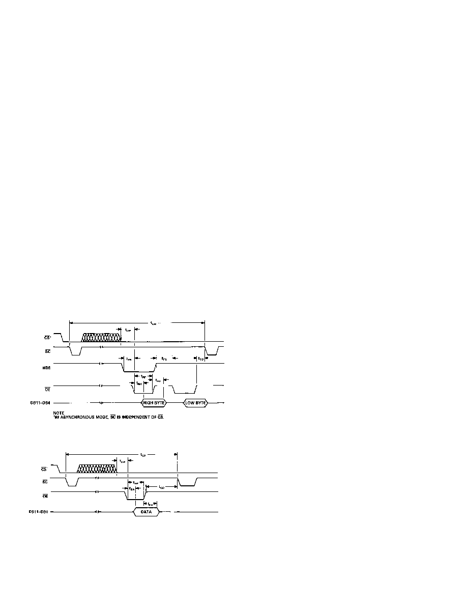
Figure 10 illustrates the 8-bit read mode (12/
8 = LOW), where
only DB11–DB4 are used as output lines onto an 8-bit bus. The
output is read in two steps, with the high byte read first, followed
by the low byte. High Byte Enable (
HBE) controls the output
sequence. The 12-bit result can be right or left justified depend-
ing on the state of R/
L.
In 12-bit read mode (12/
8 = HIGH), a single READ operation
accesses all 12 output bits on DB11-DB0 for interface to a
16-bit bus. Figure 11 provides the output timing relationships.
Note that tCR must be observed, in that SC pulses should not be
issued at intervals closer than 5
s. If SC is asserted sooner than
5
s, conversion accuracy may deteriorate. For this reason, SC
should not be held LOW in an attempt to operate in a continu-
ously converting mode.
Figure 10. Output Timing, 8-Bit Read Mode
NOTE
1IN ASYNCHRONOUS MODE,
SC IS INDEPENDENT OF CS
Figure 11. Output Timing, 12-Bit Read Mode
POWER-UP
The AD678 typically requires 10
s after power-up to reset
internal logic.
APPLICATION INFORMATION
INPUT CONNECTIONS AND CALIBRATION
The high (10 M
) input impedance of the AD678 eases the
task of interfacing to high source impedances or multiplexer
channel-to-channel mismatches of up to 1000
. The 10 V p-p
full-scale input range accepts the majority of signal voltages
without the need for voltage divider networks which could dete-
riorate the accuracy of the ADC.
The AD678 is factory trimmed to minimize linearity, offset and
gain errors. In unipolar mode, the only external component that
is required is a 50
± 1% resistor. Two resistors are required in
bipolar mode. If offset and gain are not critical (as in some ac
applications), even these components can be eliminated.
In some applications, offset and gain errors need to be trimmed
out completely. The following sections describe the correct pro-
cedure for these various situations.
UNIPOLAR RANGE INPUTS
Offset and gain errors can be trimmed out by using the configu-
ration shown in Figure 12. This circuit allows approximately
±25 mV of offset trim range (±10 LSB) and ±0.5% of gain trim
(
±20 LSB).
The first transition (from 0000 0000 0000 to 0000 0000 0001)
should nominally occur for an input level of +1/2 LSB (1.22 mV
above ground for a 10 V range). To trim unipolar zero to this
nominal value, apply a 1.22 mV signal to AIN and adjust R1
until the first transition is located.
The gain trim is done by adjusting R2. If the nominal value is
required, apply a signal 1 1/2 LSB below full scale (9.9963 V for
a 10 V range) and adjust R2 until the last transition is located
(1111 1111 1110 to 1111 1111 1111).
If offset adjustment is not required, BIPOFF should be con-
nected directly to AGND. If gain adjustment is not required, R2
should be replaced with a fixed 50
± 1% metal film resistor. If
REFOUT is connected directly to REFIN, the additional gain
error will be approximately 1%.
BIPOLAR RANGE INPUTS
The connections for the bipolar mode are shown in Figure 13.
In this mode, data output coding will be in twos complement
binary. This circuit will allow approximately
±25 mV of offset
trim range (
±10 LSB) and ±0.5% of gain trim range (20 LSB).
Either or both of the trim pots can be replaced with 50
± 1%
fixed resistors if the AD678 accuracy limits are sufficient for the
application. If the pins are shorted together, the additional offset
and gain errors will be approximately 1%.
To trim bipolar zero to its nominal value, apply a signal 1/2 LSB
below midrange (–1.22 mV for a
±5 V range) and adjust R1
until the major carry transition is located (1111 1111 1111 to
0000 0000 0000). To trim the gain, apply a signal 1 1/2 LSB
below full scale (+4.9963 V for a
±5 V range) and adjust R2 to
give the last positive transition (0111 1111 1110 to 0111 1111
1111). These trims are interactive so several iterations may be
necessary for convergence.
相关PDF资料 |
PDF描述 |
|---|---|
| IDT72V3611L15PF8 | IC FIFO SYNC 64X36 15NS 120-TQFP |
| MS27468T21A16P | CONN RCPT 16POS JAM NUT W/PINS |
| MS27468E21A16P | CONN RCPT 16POS JAM NUT W/PINS |
| IDT72821L15PF | IC FIFO SYNC 1KX9 15NS 64QFP |
| AD6654CBCZ | IC ADC 14BIT W/4CH RSP 256CSPBGA |
相关代理商/技术参数 |
参数描述 |
|---|---|
| AD678BD | 功能描述:IC ADC 12BIT SAMPLING 28-CDIP RoHS:否 类别:集成电路 (IC) >> 数据采集 - 模数转换器 系列:- 产品培训模块:Lead (SnPb) Finish for COTS Obsolescence Mitigation Program 标准包装:250 系列:- 位数:12 采样率(每秒):1.8M 数据接口:并联 转换器数目:1 功率耗散(最大):1.82W 电压电源:模拟和数字 工作温度:-40°C ~ 85°C 安装类型:表面贴装 封装/外壳:48-LQFP 供应商设备封装:48-LQFP(7x7) 包装:管件 输入数目和类型:2 个单端,单极 |
| AD678BJ | 功能描述:IC ADC 12BIT SAMPLING 44-JLCC RoHS:否 类别:集成电路 (IC) >> 数据采集 - 模数转换器 系列:- 产品培训模块:Lead (SnPb) Finish for COTS Obsolescence Mitigation Program 标准包装:2,500 系列:- 位数:12 采样率(每秒):3M 数据接口:- 转换器数目:- 功率耗散(最大):- 电压电源:- 工作温度:- 安装类型:表面贴装 封装/外壳:SOT-23-6 供应商设备封装:SOT-23-6 包装:带卷 (TR) 输入数目和类型:- |
| AD678JD | 功能描述:IC ADC 12BIT SAMPLING 28-CDIP RoHS:否 类别:集成电路 (IC) >> 数据采集 - 模数转换器 系列:- 产品培训模块:Lead (SnPb) Finish for COTS Obsolescence Mitigation Program 标准包装:250 系列:- 位数:12 采样率(每秒):1.8M 数据接口:并联 转换器数目:1 功率耗散(最大):1.82W 电压电源:模拟和数字 工作温度:-40°C ~ 85°C 安装类型:表面贴装 封装/外壳:48-LQFP 供应商设备封装:48-LQFP(7x7) 包装:管件 输入数目和类型:2 个单端,单极 |
| AD678JN | 制造商:Analog Devices 功能描述:ADC Single Flash 200ksps 12-bit Parallel 28-Pin PDIP W 制造商:Rochester Electronics LLC 功能描述:IC - 12-BIT SAMPLING ADC - Bulk 制造商:Analog Devices 功能描述:SEMICONDUCTORSLINEAR ((NS)) |
| AD678JNZ | 功能描述:IC ADC 12BIT SAMPLING 28-DIP RoHS:是 类别:集成电路 (IC) >> 数据采集 - 模数转换器 系列:- 标准包装:1 系列:- 位数:14 采样率(每秒):83k 数据接口:串行,并联 转换器数目:1 功率耗散(最大):95mW 电压电源:双 ± 工作温度:0°C ~ 70°C 安装类型:通孔 封装/外壳:28-DIP(0.600",15.24mm) 供应商设备封装:28-PDIP 包装:管件 输入数目和类型:1 个单端,双极 |
发布紧急采购,3分钟左右您将得到回复。