参数资料
| 型号: | AD708JNZ |
| 厂商: | Analog Devices Inc |
| 文件页数: | 3/16页 |
| 文件大小: | 0K |
| 描述: | IC OPAMP GP DUAL PREC 8DIP |
| 标准包装: | 50 |
| 放大器类型: | 通用 |
| 电路数: | 2 |
| 转换速率: | 0.3 V/µs |
| -3db带宽: | 900kHz |
| 电流 - 输入偏压: | 1nA |
| 电压 - 输入偏移: | 30µV |
| 电流 - 电源: | 4.5mA |
| 电压 - 电源,单路/双路(±): | 6 V ~ 36 V,±3 V ~ 18 V |
| 工作温度: | 0°C ~ 70°C |
| 安装类型: | 通孔 |
| 封装/外壳: | 8-DIP(0.300",7.62mm) |
| 供应商设备封装: | 8-PDIP |
| 包装: | 管件 |
| 产品目录页面: | 766 (CN2011-ZH PDF) |
AD708
Rev. C | Page 11 of 16
OPERATION WITH A GAIN OF 100
To show the outstanding dc precision of the AD708 in a real
application, Table 3 shows an error budget calculation for a gain
of 100. This configuration is shown in Figure 28.
Table 3.
Error Sources
Maximum Error Contribution
AV = 100 (S Grade)
(Full Scale: VOUT = 10 V, VIN = 100 mV)
VOS
30 μV/100 mV
= 300 ppm
IOS
(100 kΩ)(1 nA)/10 V
= 10 ppm
Gain (2 kΩ Load)
10 V/(5 × 106)/100 mV
= 20 ppm
Noise
0.35 mV/100 mV
= 4 ppm
VOS Drift
(0.3 mV/°C)/100 mV
= 3 ppm/°C
Total Unadjusted
Error
@ 25°C
= 334 ppm > 11 bits
55°C to +125°C
= 634 ppm > 10 bits
With Offset
Calibrated Out
@ 25°C
= 34 ppm > 14 bits
55°C to +125°C
= 334 ppm > 11 bits
1/2
AD708
VOUT
VIN
+
–
100k
1k
2
3
7
4
6
0.1F
+VS
–VS
0
578
9-
0
28
Figure 28. Gain of 100 Configuration
This error budget assumes no error in the resistor ratio and no
error from power supply variation (the 120 dB minimum PSRR
of the AD708S makes this a good assumption). The external
resistors can cause gain error from mismatch and drift over
temperature.
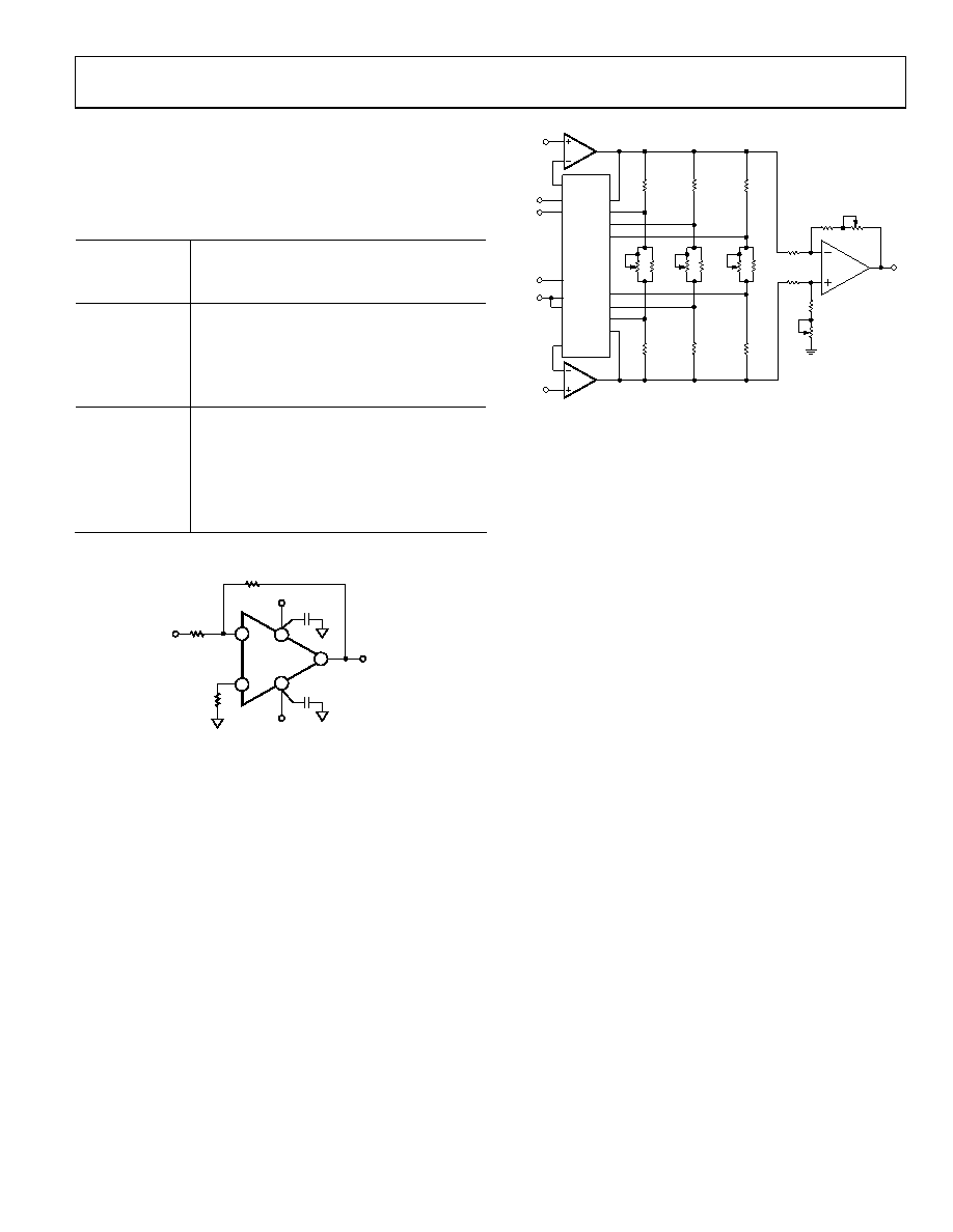
HIGH PRECISION PROGRAMMABLE GAIN
AMPLIFIER
The three op amp programmable gain amplifier shown in
Figure 29 takes advantage of the outstanding matching
characteristics of the AD708 to achieve high dc precision.
0
578
9-
02
9
S1
S2
A0
A1
S3
S4
S8
S7
+VS
–VS
S6
S5
AD7502
OUT
1–4
OUT
5–8
1/2
AD708
VINA
1/2
AD708
VINB
10k
26.
1
100
10k
26.
1
1k
10k
26.
1
10k
AD707
10k
9.9k
RA
9.9k
RB
Figure 29. Precision PGA
The gains of the circuit are controlled by the select lines, A0 and
A1, of the AD7502 multiplexer, and are 1, 10, 100, and 1000 in
this design.
The input stage attains very high dc precision due to the 30 μV
maximum offset voltage match of the AD708S and the 1 nA
maximum input bias current match. The accuracy is main-
tained over temperature because of the ultralow drift
performance of the AD708.
To achieve 0.1% gain accuracy, along with high common-mode
rejection, the circuit should be trimmed.
To maximize common-mode rejection
1.
Set the select lines for gain = 1 and ground VINB.
2.
Apply a precision dc voltage to VINA and trim RA until
VO = VINA to the required precision.
3.
Connect VINB to VINA and apply an input voltage equal to
the full-scale common mode expected.
4.
Trim RB until V
B
O
= 0 V.
To minimize gain errors
1.
Select gain = 10 with the control lines and apply a
differential input voltage.
2.
Adjust the 100 Ω potentiometer to VO = 10 VIN
(adjust VIN magnitude as necessary).
3.
Repeat Step 1 and Step 2 for gain = 100 and gain = 1000,
adjusting the 1 kΩ and 10 kΩ potentiometers, respectively.
The design shown in Figure 29 should allow for 0.1% gain
accuracy and 0.1 μV/V common-mode rejection when ±1%
resistors and ±5% potentiometers are used.
相关PDF资料 |
PDF描述 |
|---|---|
| LT1112ACN8#PBF | IC PREC OP-AMP LOWPWR DUAL 8-DIP |
| TMM-150-01-S-D | CONN HEADER 100POS DUAL 2MM T/H |
| LT1079CN#PBF | IC PREC OPAMP MICRPWR QUAD 14DIP |
| LT6600IS8-20#PBF | IC AMP DIFF LP FLTR 20MHZ 8-SOIC |
| LT1361CS8#PBF | IC OP-AMP HI-SPD 50MHZ DUAL8SOIC |
相关代理商/技术参数 |
参数描述 |
|---|---|
| AD708JQ | 制造商:未知厂家 制造商全称:未知厂家 功能描述:Voltage-Feedback Operational Amplifier |
| AD708KH | 制造商:未知厂家 制造商全称:未知厂家 功能描述:Voltage-Feedback Operational Amplifier |
| AD708KN | 制造商:未知厂家 制造商全称:未知厂家 功能描述:Voltage-Feedback Operational Amplifier |
| AD708KQ | 制造商:未知厂家 制造商全称:未知厂家 功能描述:Voltage-Feedback Operational Amplifier |
| AD708SGRADECHIPS | 制造商:AD 制造商全称:Analog Devices 功能描述:Ultralow Offset Voltage Dual Op Amp |
发布紧急采购,3分钟左右您将得到回复。