参数资料
| 型号: | AD708JNZ |
| 厂商: | Analog Devices Inc |
| 文件页数: | 4/16页 |
| 文件大小: | 0K |
| 描述: | IC OPAMP GP DUAL PREC 8DIP |
| 标准包装: | 50 |
| 放大器类型: | 通用 |
| 电路数: | 2 |
| 转换速率: | 0.3 V/µs |
| -3db带宽: | 900kHz |
| 电流 - 输入偏压: | 1nA |
| 电压 - 输入偏移: | 30µV |
| 电流 - 电源: | 4.5mA |
| 电压 - 电源,单路/双路(±): | 6 V ~ 36 V,±3 V ~ 18 V |
| 工作温度: | 0°C ~ 70°C |
| 安装类型: | 通孔 |
| 封装/外壳: | 8-DIP(0.300",7.62mm) |
| 供应商设备封装: | 8-PDIP |
| 包装: | 管件 |
| 产品目录页面: | 766 (CN2011-ZH PDF) |
AD708
Rev. C | Page 12 of 16
BRIDGE SIGNAL CONDITIONER
The AD708 can be used in the circuit shown in Figure 30 to
produce an accurate and inexpensive dynamic bridge condi-
tioner. The low offset voltage match and low offset voltage drift
match of the AD708 combine to achieve circuit performance
better than all but the best instrumentation amplifiers. The
outstanding specifications of the AD708, such as open-loop
gain, input offset currents, and low input bias currents, do not
limit circuit accuracy.
As configured, the circuit only requires a gain resistor, RG, of
suitable accuracy and a stable, accurate voltage reference. The
transfer function is
VO = VREF [ΔR/(R + ΔR)][RG/R]
The only significant errors due to the AD708S are
VOS_OUT = (VOS_MATCH)(2RG/R) = 30 mV
VOS_OUT (T) = (VOS_DRIFT)(2RG/R) = 0.3 mV/°C
To achieve high accuracy, Resistor RG should be 0.1% or better
with a low drift coefficient.
0
57
89
-0
30
R
R = 350
R + ΔR
1/2
AD708
VO
–15V
RG
175k
1/2
AD708
887
VREF
+15V
AD580
2.5V
Figure 30. Bridge Signal Conditioning Circuit
05
78
9-
03
1
IN4591
NOTE
1LOW LEAKAGE DIODES
1/2
AD708
1/2
AD708
5k
10k
VIN
VO = |VIN|
10k
5k
3.75k
10k
Figure 31. Precision Absolute Value Circuit
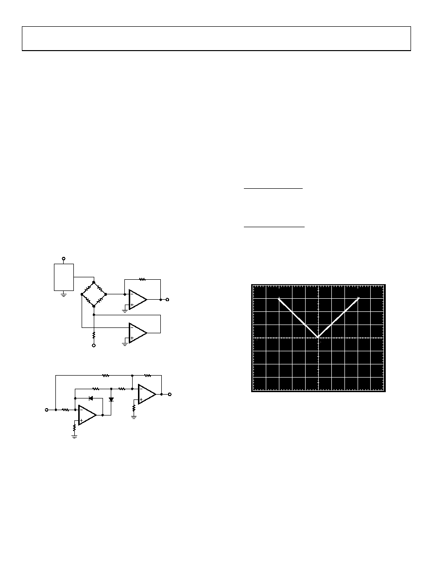
PRECISION ABSOLUTE VALUE CIRCUIT
The AD708 is ideally suited to the precision absolute value
circuit shown in Figure 31. The low offset voltage match of the
AD708 enables this circuit to accurately resolve the input signal.
In addition, the tight offset voltage drift match maintains the
resolution of the circuit over the full military temperature
range. The high dc open-loop gain and exceptional gain
linearity allows the circuit to perform well at both large and
small signal levels.
In this circuit, the only significant dc errors are due to the offset
voltage of the two amplifiers, the input offset current match of
the amplifiers, and the mismatch of the resistors. Errors
associated with the AD708S contribute less than 0.001% error
over 55°C to +125°C.
Maximum error at 25°C
(
)( )
ppm
4
μV
μV/10
40
V
10
nA
1
kΩ
10
μV
30
=
+
Maximum error at +125°C or 55°C
(
)(
)
C
125
@
ppm
7
V
10
kΩ
10
nA
2
μV
50
°
+
=
+
signal at 0.05 Hz. Note that the circuit exhibits very low offset at
the zero crossing. This circuit can also produce VOUT = |VIN| by
reversing the polarity of the two diodes.
05
78
9-
03
2
VIN = 1mV/DIV
V
OU
T=
1m
V/
D
IV
1mV
Figure 32. Absolute Value Circuit Performance
(Input Signal = 0.05 Hz)
SELECTION OF PASSIVE COMPONENTS
Use high quality passive components to take full advantage of
the high precision and low drift characteristics of the AD708.
Discrete resistors and resistor networks with temperature
coefficients of less than 10 ppm/°C are available from Vishay,
Caddock, Precision Replacement Parts (PRP), and others.
相关PDF资料 |
PDF描述 |
|---|---|
| LT1112ACN8#PBF | IC PREC OP-AMP LOWPWR DUAL 8-DIP |
| TMM-150-01-S-D | CONN HEADER 100POS DUAL 2MM T/H |
| LT1079CN#PBF | IC PREC OPAMP MICRPWR QUAD 14DIP |
| LT6600IS8-20#PBF | IC AMP DIFF LP FLTR 20MHZ 8-SOIC |
| LT1361CS8#PBF | IC OP-AMP HI-SPD 50MHZ DUAL8SOIC |
相关代理商/技术参数 |
参数描述 |
|---|---|
| AD708JQ | 制造商:未知厂家 制造商全称:未知厂家 功能描述:Voltage-Feedback Operational Amplifier |
| AD708KH | 制造商:未知厂家 制造商全称:未知厂家 功能描述:Voltage-Feedback Operational Amplifier |
| AD708KN | 制造商:未知厂家 制造商全称:未知厂家 功能描述:Voltage-Feedback Operational Amplifier |
| AD708KQ | 制造商:未知厂家 制造商全称:未知厂家 功能描述:Voltage-Feedback Operational Amplifier |
| AD708SGRADECHIPS | 制造商:AD 制造商全称:Analog Devices 功能描述:Ultralow Offset Voltage Dual Op Amp |
发布紧急采购,3分钟左右您将得到回复。