参数资料
| 型号: | AD7111BQ |
| 厂商: | Analog Devices Inc |
| 文件页数: | 6/8页 |
| 文件大小: | 0K |
| 描述: | IC DAC LOGARITHMIC 16-CDIP |
| 产品培训模块: | Data Converter Fundamentals DAC Architectures |
| 标准包装: | 1 |
| 系列: | LOGDAC® |
| 位数: | 17 |
| 转换器数目: | 1 |
| 电压电源: | 单电源 |
| 功率耗散(最大): | 1W |
| 工作温度: | -40°C ~ 85°C |
| 安装类型: | 通孔 |
| 封装/外壳: | 16-CDIP(0.300",7.62mm) |
| 供应商设备封装: | 16-CDIP |
| 包装: | 管件 |
| 输出数目和类型: | 1 电流,单极 |
| 采样率(每秒): | * |
AD7111/AD7111A
REV. 0
–6–
For example, the AD7111L is guaranteed monotonic in 0.375 dB
steps from 0 dB to –54 dB inclusive and in 0.75 dB steps from
0 dB to –72 dB inclusive. To achieve monotonic operation over
the entire 88.5 dB range it is necessary to select input codes so
that the attenuation step size at any point is consistent with the
step size guaranteed for monotonic operation at that point.
EQUIVALENT CIRCUIT ANALYSIS
Figure 2 shows a simplified circuit of the D/A converter section
of the AD7111/AD7111A, and Figure 3 gives an approximate
equivalent circuit.
The current source ILEAKAGE is composed of surface and junc-
tion leakages. The resistor R0 as shown in Figure 3 is the
equivalent output resistance of the device which varies with in-
put code (excluding all 0s code) from 0.8R to 2R. R is typically
12 k
. C
OUT is the capacitance due to the N channel switches
and varies from about 20 pF to 50 pF depending upon the digi-
tal input. For further information on CMOS multiplying D/A
converters, refer to “CMOS DAC Application Guide” which is
available from Analog Devices, Publication Number
G872b–8–1/89.
Figure 2. Simplified D/A Circuit of AD7111/AD7111A
Figure 3. Equivalent Analog Output Circuit of
AD7111/AD7111A
DYNAMIC PERFORMANCE
The dynamic performance of the AD7111/AD7111A will depend
upon the gain and phase characteristics of the output amplifier,
together with the optimum choice of PC board layout and
decoupling components. Circuit layout is most important if the
optimum performance of the AD7111/AD7111A is to be
achieved. Most application problems stem from either poor lay-
out, grounding errors, or inappropriate choice of amplifier.
It is recommended that when using thc AD7111/AD7111A with
a high speed amplifier, a capacitor (C1) he connected in the
feedback path as shown in Figure 1. This capacitor, which
should be between 10 pF and 30 pF, compensates for the phase
lag introduced by the output capacitance of the D/A converter.
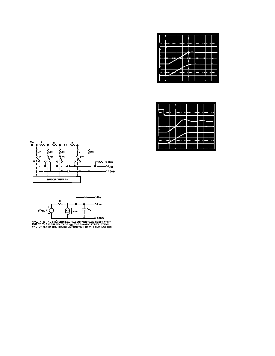
Figures 4 and 5 show the performance of the AD7111/AD7111A
using the AD711, a high speed, low cost BiFET amplifier, and
the OP275, a dual, bipolar/JFET, audio amplifier. The perfor-
mance without C1 is shown in the middle trace and the re-
sponse with C1 in circuit shown in the bottom trace.
10
90
100
0%
A1
–0.2V
200ns
5V
V
OUT
V
OUT
C1 = 0pF
C1 = 15pF
DATA CHANGE
MSB
DATA CHANGE FROM 80H TO 00H.
Figure 4. Response of AD7111/AD7111A with AD711
10
90
100
0%
A1
200ns
5V
V
OUT
V
OUT
C1 = 0pF
C1 = 15pF
DATA CHANGE
MSB
DATA CHANGE FROM 80H TO 00H.
0.4V
Figure 5. Response of AD7111/AD7111A with 1/2 OP275
In conventional CMOS D/A converter design, parasitic capaci-
tance in N-channel D/A converter switches can give rise to
glitches on the D/A converter output. These glitches result from
digital feedthrough. The AD7111/AD7111A has been designed
to minimize these glitches as much as possible.
For operation beyond 250 kHz, capacitor C1 may be reduced in
value. This gives an increase in bandwidth at the expense of a
poorer transient response as shown in Figures 5 and 11. In cir-
cuits where C1 is not included, the high frequency roll-off point
is primarily determined by the characteristics of the output am-
plifier and not the AD7111/AD7111A.
Feedthrough and absolute accuracy are sensitive to output leak-
age current effects. For this reason it is recommended that the
operating temperature of the AD7111/AD7111A be kept as
close to 25
°C as is practically possible, particularly where the
device’s performance at high attenuation levels is important. A typi-
cal plot of leakage current vs. temperature is shown in Figure 10.
Some solder fluxes and cleaning materials can form slightly con-
ductive films which cause leakage effects between analog
input and output. The user is cautioned to ensure that the
manufacturing process for circuits using thc AD7111/AD7111A
does not allow such films to form. Otherwise the feedthrough,
accuracy and maximum usable range will be affected.
STATIC ACCURACY PERFORMANCE
The D/A converter section of the AD7111/AD7111A consists of
a 17-bit R-2R type converter. To obtain optimum static perfor-
mance at this level of resolution it is necessary to pay great
attention to amplifier selection, circuit grounding, etc.
Amplifier input has current results in a dc offset at the output of
the amplifier due to the current flowing through the feedback
resistor RFB. It is recommended that an amplifier with an input
bias current of less than 10 nA be used (e.g., AD711) to mini-
mize this offset.
相关PDF资料 |
PDF描述 |
|---|---|
| AD7170BCPZ-REEL7 | IC ADC 12BIT SIGMA-DELTA 10LFCSP |
| AD7171BCPZ-REEL7 | IC ADC 16BIT SER 125HZ 10LFCSP |
| AD7190BRUZ-REEL | IC ADC 2CH 24BIT W/PGA 24TSSOP |
| AD7191BRUZ | IC ADC 2CH 24B SD 24TSSOP |
| AD7192BRUZ | IC ADC 24BIT 2CH W/PGA 24-TSSOP |
相关代理商/技术参数 |
参数描述 |
|---|---|
| AD7111CQ | 制造商:AD 制造商全称:Analog Devices 功能描述:LC2MOS LOGDAC Logarithmic D/A Converter |
| AD7111KN | 功能描述:IC DAC LOGARITHMIC 16-DIP RoHS:否 类别:集成电路 (IC) >> 数据采集 - 数模转换器 系列:LOGDAC® 标准包装:2,400 系列:- 设置时间:- 位数:18 数据接口:串行 转换器数目:3 电压电源:模拟和数字 功率耗散(最大):- 工作温度:-40°C ~ 85°C 安装类型:表面贴装 封装/外壳:36-TFBGA 供应商设备封装:36-TFBGA 包装:带卷 (TR) 输出数目和类型:* 采样率(每秒):* |
| AD7111KNZ | 功能描述:IC DAC MONO MULTIPLYING 16DIP RoHS:是 类别:集成电路 (IC) >> 数据采集 - 数模转换器 系列:LOGDAC® 产品培训模块:Lead (SnPb) Finish for COTS Obsolescence Mitigation Program 标准包装:1,000 系列:- 设置时间:1µs 位数:8 数据接口:串行 转换器数目:8 电压电源:双 ± 功率耗散(最大):941mW 工作温度:0°C ~ 70°C 安装类型:表面贴装 封装/外壳:24-SOIC(0.295",7.50mm 宽) 供应商设备封装:24-SOIC W 包装:带卷 (TR) 输出数目和类型:8 电压,单极 采样率(每秒):* |
| AD7111LN | 功能描述:IC DAC LOGARITHMIC 16-DIP RoHS:否 类别:集成电路 (IC) >> 数据采集 - 数模转换器 系列:LOGDAC® 标准包装:2,400 系列:- 设置时间:- 位数:18 数据接口:串行 转换器数目:3 电压电源:模拟和数字 功率耗散(最大):- 工作温度:-40°C ~ 85°C 安装类型:表面贴装 封装/外壳:36-TFBGA 供应商设备封装:36-TFBGA 包装:带卷 (TR) 输出数目和类型:* 采样率(每秒):* |
| AD7111LNZ | 功能描述:IC DAC MONO MULTIPLYING 16DIP RoHS:是 类别:集成电路 (IC) >> 数据采集 - 数模转换器 系列:LOGDAC® 标准包装:1 系列:- 设置时间:4.5µs 位数:12 数据接口:串行,SPI? 转换器数目:1 电压电源:单电源 功率耗散(最大):- 工作温度:-40°C ~ 125°C 安装类型:表面贴装 封装/外壳:8-SOIC(0.154",3.90mm 宽) 供应商设备封装:8-SOICN 包装:剪切带 (CT) 输出数目和类型:1 电压,单极;1 电压,双极 采样率(每秒):* 其它名称:MCP4921T-E/SNCTMCP4921T-E/SNRCTMCP4921T-E/SNRCT-ND |
发布紧急采购,3分钟左右您将得到回复。