参数资料
| 型号: | AD7111BQ |
| 厂商: | Analog Devices Inc |
| 文件页数: | 7/8页 |
| 文件大小: | 0K |
| 描述: | IC DAC LOGARITHMIC 16-CDIP |
| 产品培训模块: | Data Converter Fundamentals DAC Architectures |
| 标准包装: | 1 |
| 系列: | LOGDAC® |
| 位数: | 17 |
| 转换器数目: | 1 |
| 电压电源: | 单电源 |
| 功率耗散(最大): | 1W |
| 工作温度: | -40°C ~ 85°C |
| 安装类型: | 通孔 |
| 封装/外壳: | 16-CDIP(0.300",7.62mm) |
| 供应商设备封装: | 16-CDIP |
| 包装: | 管件 |
| 输出数目和类型: | 1 电流,单极 |
| 采样率(每秒): | * |
AD7111/AD7111A
REV. 0
–7–
Another error arises from the output amplifier s input offset
voltage. The amplifier is operated with a fixed feedback resis-
tance, but the equivalent source impedance (the AD7111/
AD7111A output impedance) varies as a function of attenuation
level. This has the effect of varying thc “noise” gain of the
amplifier, thus creating a varying error due to amplifier offset
voltage. It is recommended that an amplifier with less than
50
V of input offset be used (such as the AD OP07 in dc appli-
cations. Amplifiers with higher offset voltage may cause audible
“thumps” in ac applications due to dc output changes.
The AD7111/AD7111A accuracy is specified and tested using
only the internal feedback resistor. Any gain error (i.e., mis-
match of RFB to the R-2R ladder) that may exist in the
AD7111/AD7111A D/A converter circuit results in a constant
attenuation error over the whole range. The AD7111/AD7111A
accuracy is specified relative to 0 dB attenuation, hence “Gain”
trim resistors—R1 and R2 in Figure 1—can be used to adjust
VOUT = VIN precisely (i.e., 0 dB attenuation) with input code
00000000. The accuracy and monotonic range specifications of
the AD7111/AD7111A are not affected in any way by this gain
trim procedure. For the AD7111/AD7111A L/C/U grades, suit-
able values for R1 and R2 of Figure 1 are R1 = 500
, R2 =
180
; for the K/B/T grades, suitable value are R1 = 1000 ,
R2 = 270
. For additional information on gain error the reader
is referred to the “CMOS DAC Application Guide,” available
from Analog Devices, Inc., Publication Number G872b–8–1/89.
Typical Performance Characteristics
6
0
5
3
1
2
0
5
4
3
2
INPUT VOLTAGE – Volts
I
DD
–
mA
V
IN APPLIED TO ALL DATA INPUTS
V
DD = +5V
T
A = +25°C
CS = WR = 0V
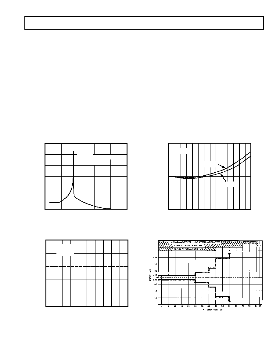
Figure 6. Typical Supply Current vs. Logic Input Level
0.4
–0.6
30
0.0
–0.4
3
–0.2
0
0.2
27
24
21
18
15
12
9
6
ATTENUATION – dB
ERROR
–
dB
* *
* * *
* *
*
* *
* * *
**
*
* ** *
**
*
* *
* * * * **
*
* * *
* *
*
V
DD = +5V
T
A = +25
°C
Figure 7. Typical Attenuation Error for 0.75 dB Steps
1.0
–1.0
078
0.5
–0.5
6
0.0
66
72
60
48
42
36
30
24
18
12
54
84
ATTENUATION – dB
ERROR
–
dB
T
A = +85
°C
T
A = +25
°C
DD
V
= +5V
Figure 8. Typical Attenuation Error for 3 dB Steps vs.
Temperature
Figure 9. Accuracy Specification for K/B/T Grade Devices
at TA = +25°C
相关PDF资料 |
PDF描述 |
|---|---|
| AD7170BCPZ-REEL7 | IC ADC 12BIT SIGMA-DELTA 10LFCSP |
| AD7171BCPZ-REEL7 | IC ADC 16BIT SER 125HZ 10LFCSP |
| AD7190BRUZ-REEL | IC ADC 2CH 24BIT W/PGA 24TSSOP |
| AD7191BRUZ | IC ADC 2CH 24B SD 24TSSOP |
| AD7192BRUZ | IC ADC 24BIT 2CH W/PGA 24-TSSOP |
相关代理商/技术参数 |
参数描述 |
|---|---|
| AD7111CQ | 制造商:AD 制造商全称:Analog Devices 功能描述:LC2MOS LOGDAC Logarithmic D/A Converter |
| AD7111KN | 功能描述:IC DAC LOGARITHMIC 16-DIP RoHS:否 类别:集成电路 (IC) >> 数据采集 - 数模转换器 系列:LOGDAC® 标准包装:2,400 系列:- 设置时间:- 位数:18 数据接口:串行 转换器数目:3 电压电源:模拟和数字 功率耗散(最大):- 工作温度:-40°C ~ 85°C 安装类型:表面贴装 封装/外壳:36-TFBGA 供应商设备封装:36-TFBGA 包装:带卷 (TR) 输出数目和类型:* 采样率(每秒):* |
| AD7111KNZ | 功能描述:IC DAC MONO MULTIPLYING 16DIP RoHS:是 类别:集成电路 (IC) >> 数据采集 - 数模转换器 系列:LOGDAC® 产品培训模块:Lead (SnPb) Finish for COTS Obsolescence Mitigation Program 标准包装:1,000 系列:- 设置时间:1µs 位数:8 数据接口:串行 转换器数目:8 电压电源:双 ± 功率耗散(最大):941mW 工作温度:0°C ~ 70°C 安装类型:表面贴装 封装/外壳:24-SOIC(0.295",7.50mm 宽) 供应商设备封装:24-SOIC W 包装:带卷 (TR) 输出数目和类型:8 电压,单极 采样率(每秒):* |
| AD7111LN | 功能描述:IC DAC LOGARITHMIC 16-DIP RoHS:否 类别:集成电路 (IC) >> 数据采集 - 数模转换器 系列:LOGDAC® 标准包装:2,400 系列:- 设置时间:- 位数:18 数据接口:串行 转换器数目:3 电压电源:模拟和数字 功率耗散(最大):- 工作温度:-40°C ~ 85°C 安装类型:表面贴装 封装/外壳:36-TFBGA 供应商设备封装:36-TFBGA 包装:带卷 (TR) 输出数目和类型:* 采样率(每秒):* |
| AD7111LNZ | 功能描述:IC DAC MONO MULTIPLYING 16DIP RoHS:是 类别:集成电路 (IC) >> 数据采集 - 数模转换器 系列:LOGDAC® 标准包装:1 系列:- 设置时间:4.5µs 位数:12 数据接口:串行,SPI? 转换器数目:1 电压电源:单电源 功率耗散(最大):- 工作温度:-40°C ~ 125°C 安装类型:表面贴装 封装/外壳:8-SOIC(0.154",3.90mm 宽) 供应商设备封装:8-SOICN 包装:剪切带 (CT) 输出数目和类型:1 电压,单极;1 电压,双极 采样率(每秒):* 其它名称:MCP4921T-E/SNCTMCP4921T-E/SNRCTMCP4921T-E/SNRCT-ND |
发布紧急采购,3分钟左右您将得到回复。