参数资料
| 型号: | AD711KRZ |
| 厂商: | Analog Devices Inc |
| 文件页数: | 15/16页 |
| 文件大小: | 0K |
| 描述: | IC OPAMP BIFET PREC 25MA 8SOIC |
| 产品培训模块: | Op Amp Basics |
| 标准包装: | 98 |
| 放大器类型: | J-FET |
| 电路数: | 1 |
| 转换速率: | 20 V/µs |
| -3db带宽: | 4MHz |
| 电流 - 输入偏压: | 15pA |
| 电压 - 输入偏移: | 200µV |
| 电流 - 电源: | 2.5mA |
| 电流 - 输出 / 通道: | 25mA |
| 电压 - 电源,单路/双路(±): | 9 V ~ 36 V,±4.5 V ~ 18 V |
| 工作温度: | 0°C ~ 70°C |
| 安装类型: | 表面贴装 |
| 封装/外壳: | 8-SOIC(0.154",3.90mm 宽) |
| 供应商设备封装: | 8-SOIC |
| 包装: | 管件 |
| 产品目录页面: | 773 (CN2011-ZH PDF) |
REV. E
AD711
–8–
OP AMP SETTLING TIME—A MATHEMATICAL MODEL
The design of the AD711 gives careful attention to optimizing
individual circuit components; in addition, a careful tradeoff was
made: the gain bandwidth product (4 MHz) and slew rate
(20 V/
ms) were chosen to be high enough to provide very fast
settling time but not too high to cause a significant reduction in
phase margin (and therefore stability). Thus designed, the AD711
settles to
±0.01%, with a 10 V output step, in under 1 ms, while
retaining the ability to drive a 100 pF load capacitance when
operating as a unity gain follower.
If an op amp is modeled as an ideal integrator with a unity gain
crossover frequency of
wo/2p, Equation 1 will accurately describe
the small signal behavior of the circuit of Figure 3a, consisting of
an op amp connected as an I-to-V converter at the output of a
bipolar or CMOS DAC. This equation would completely describe
the output of the system if not for the op amp’s finite slew rate
and other nonlinear effects.
V
O
I
IN
=
– R
R(C
f
= C
X )
wo
s
2
+
G
N
wo +
RC
f
s
+1
(3)
where:
wo
2p
=op amp’s unity gain frequency
GN = “noise” gain of circuit 1 +
R
O
This equation may then be solved for Cf:
C
f
=
2
- G
N
R
wo +
2 RC
X
wo +(1- GN )
R
wo
(3)
In these equations, capacitor CX is the total capacitor appearing
the inverting terminal of the op amp. When modeling a DAC
buffer application, the Norton equivalent circuit of Figure 3a
can be used directly; capacitance CX is the total capacitance of
the output of the DAC plus the input capacitance of the op amp
(since the two are in parallel).
AD711
CX
RO
IO
CF
R
RL
CL
VOUT
Figure 3a. Simplified Model of the AD711 Used as a
Current-Out DAC Buffer
When RO and IO are replaced with their Thevenin VIN and RIN
equivalents, the general purpose inverting amplifier of Figure 26b
is created. Note that when using this general model, capacitance
CX is either the input capacitance of the op amp if a simple inverting
op amp is being simulated or it is the combined capacitance of
the DAC output and the op amp input if the DAC buffer is
being modeled.
AD711
CX
RIN
CF
R
RL
CL
VOUT
VIN
Figure 3b. Simplified Model of the AD711
Used as an Inverter
In either case, the capacitance CX causes the system to go from
a one-pole to a two-pole response; this additional pole increases
settling time by introducing peaking or ringing in the op amp
output. Since the value of CX can be estimated with reasonable
accuracy, Equation 2 can be used to choose a small capacitor,
CF, to cancel the input pole and optimize amplifier response.
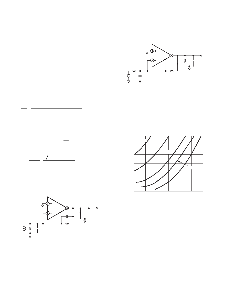
Figure 4 is a graphical solution of Equation 2 for the AD711
with R = 4 k
W.
CF
0
10
C
X
10
20
30
40
50
60
20
30
40
50
60
GN = 4.0
GN = 1.0
GN = 1.5
GN = 2.0
GN = 3.0
Figure 4. Value of Capacitor CF vs. Value of CX
The photos of Figures 5a and 5b show the dynamic response of
the AD711 in the settling test circuit of Figure 6.
The input of the settling time fixture is driven by a flat-top pulse
generator. The error signal output from the false summing node
of A1 is clamped, amplified by A2 and then clamped again. The
error signal is thus clamped twice: once to prevent overloading
amplifier A2 and then a second time to avoid overloading the
oscilloscope preamp. The Tektronix oscilloscope preamp type
7A26 was carefully chosen because it does not overload with
these input levels. Amplifier A2 needs to be a very high speed
FET-input op amp; it provides a gain of 10, amplifying the error
signal output of A1.
相关PDF资料 |
PDF描述 |
|---|---|
| PBC11SADN | CONN HEADER .100 SINGL STR 11POS |
| OP213FPZ | IC OPAMP GP 3.4MHZ DUAL LN 8DIP |
| OP213FSZ | IC OPAMP GP 3.4MHZ DUAL LN SOIC |
| PEC11SFDN | CONN HEADER .100 SINGL STR 11POS |
| 1.5SMC47AT3G | TVS 1500W 47V UNIDIRECT SMC |
相关代理商/技术参数 |
参数描述 |
|---|---|
| AD711KRZ | 制造商:Analog Devices 功能描述:IC OP-AMP 4MHZ 20V/ ((NW)) 制造商:Analog Devices 功能描述:IC, OP-AMP, 4MHZ, 20V/ us, SOIC-8 |
| AD711KRZ-REEL | 功能描述:IC OPAMP BIFET PREC 25MA 8SOIC RoHS:是 类别:集成电路 (IC) >> Linear - Amplifiers - Instrumentation 系列:- 标准包装:50 系列:LinCMOS™ 放大器类型:通用 电路数:4 输出类型:- 转换速率:0.05 V/µs 增益带宽积:110kHz -3db带宽:- 电流 - 输入偏压:0.7pA 电压 - 输入偏移:210µV 电流 - 电源:57µA 电流 - 输出 / 通道:30mA 电压 - 电源,单路/双路(±):3 V ~ 16 V,±1.5 V ~ 8 V 工作温度:-40°C ~ 85°C 安装类型:表面贴装 封装/外壳:14-SOIC(0.154",3.90mm 宽) 供应商设备封装:14-SOIC 包装:管件 产品目录页面:865 (CN2011-ZH PDF) 其它名称:296-1834296-1834-5 |
| AD711KRZ-REEL7 | 功能描述:IC OPAMP BIFET PREC 25MA 8SOIC RoHS:是 类别:集成电路 (IC) >> Linear - Amplifiers - Instrumentation 系列:- 其它有关文件:Automotive Product Guide 产品培训模块:Lead (SnPb) Finish for COTS Obsolescence Mitigation Program 标准包装:1 系列:- 放大器类型:通用 电路数:1 输出类型:满摆幅 转换速率:3 V/µs 增益带宽积:10MHz -3db带宽:- 电流 - 输入偏压:1pA 电压 - 输入偏移:70µV 电流 - 电源:2.5mA 电流 - 输出 / 通道:48mA 电压 - 电源,单路/双路(±):2.7 V ~ 5.5 V,±1.35 V ~ 2.75 V 工作温度:-40°C ~ 125°C 安装类型:表面贴装 封装/外壳:SOT-23-6 供应商设备封装:SOT-6 包装:Digi-Reel® 其它名称:MAX4475AUT#TG16DKR |
| AD711SCHIPS | 制造商:AD 制造商全称:Analog Devices 功能描述:Precision, Low Cost, High Speed, BiFET Op Amp |
| AD711SH | 制造商:AD 制造商全称:Analog Devices 功能描述:Precision, Low Cost, High Speed, BiFET Op Amp |
发布紧急采购,3分钟左右您将得到回复。