- 您现在的位置:买卖IC网 > PDF目录9489 > AD7147WPACPZ-RL (Analog Devices Inc)IC CAP-TO-DGTL CONV PROG 24LFCSP PDF资料下载
参数资料
| 型号: | AD7147WPACPZ-RL |
| 厂商: | Analog Devices Inc |
| 文件页数: | 19/73页 |
| 文件大小: | 0K |
| 描述: | IC CAP-TO-DGTL CONV PROG 24LFCSP |
| 标准包装: | 5,000 |
| 系列: | CapTouch™ |
| 类型: | 电容数字转换器 |
| 分辨率(位): | 16 b |
| 采样率(每秒): | 250k |
| 数据接口: | 串行,SPI? |
| 电压电源: | 单电源 |
| 电源电压: | 2.6 V ~ 3.6 V |
| 工作温度: | -40°C ~ 85°C |
| 安装类型: | 表面贴装 |
| 封装/外壳: | 24-VFQFN 裸露焊盘,CSP |
| 供应商设备封装: | 24-LFCSP-VQ(4x4) |
| 包装: | 带卷 (TR) |
第1页第2页第3页第4页第5页第6页第7页第8页第9页第10页第11页第12页第13页第14页第15页第16页第17页第18页当前第19页第20页第21页第22页第23页第24页第25页第26页第27页第28页第29页第30页第31页第32页第33页第34页第35页第36页第37页第38页第39页第40页第41页第42页第43页第44页第45页第46页第47页第48页第49页第50页第51页第52页第53页第54页第55页第56页第57页第58页第59页第60页第61页第62页第63页第64页第65页第66页第67页第68页第69页第70页第71页第72页第73页
Data Sheet
AD7147
Rev. D | Page 25 of 72
THRESHOLD EQUATIONS
On-Chip Logic Stage High Threshold
Y
SENSITIVIT
THRESHOLD
POS
HIGH
OFFSET
STAGEx
HIGH
OFFSET
STAGEx
HIGH
OFFSET
STAGEx
AMBIENT
SF
STAGEx
THRESHOLD
HIGH
STAGEx
_
16
4
_
4
_
×
+
+
=
(1)
On-Chip Logic Stage Low Threshold
Y
SENSITIVIT
THRESHOLD
NEG
LOW
OFFSET
STAGEx
LOW
OFFSET
STAGEx
LOW
OFFSET
STAGEx
AMBIENT
SF
STAGEx
THRESHOLD
LOW
STAGEx
_
16
4
_
4
_
×
+
+
=
(2)
CAPACITANCE SENSOR BEHAVIOR WITH
CALIBRATION
The AD7147 on-chip adaptive calibration algorithm prevents
sensor detection errors such as the one shown in Figure 36.
This is achieved by monitoring the CDC ambient levels
and readjusting the initial STAGEx_OFFSET_HIGH and
STAGEx_OFFSET_LOW values according to the amount of
ambient drift measured on each sensor. Based on the new
stage offset values, the internal STAGEx_HIGH_THRESHOLD
and STAGEx_LOW_THRESHOLD values described in
Equation 1 and Equation 2 are automatically updated.
This closed-loop routine ensures the reliability and repeatable
operation of every sensor connected to the AD7147 when they
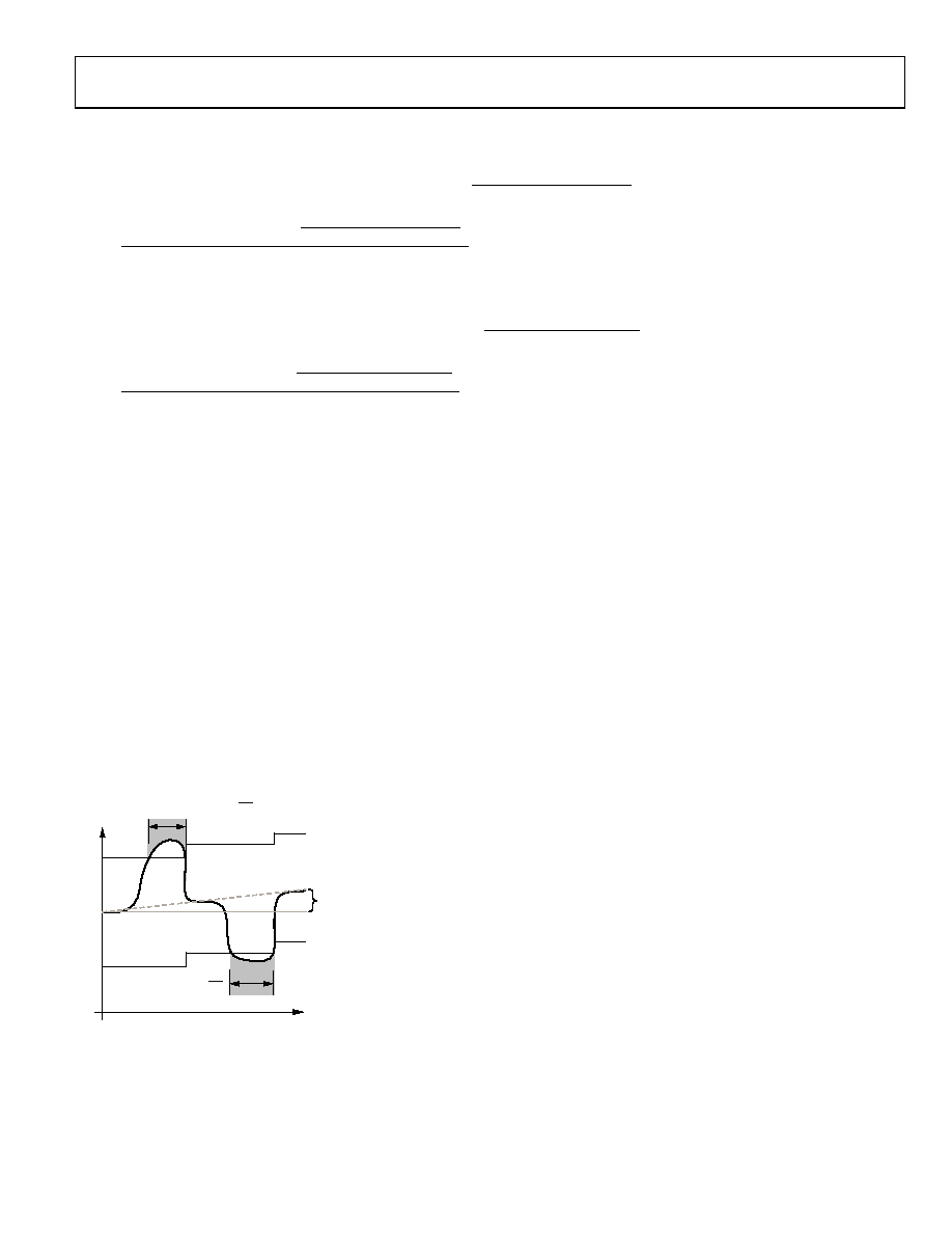
are subjected to dynamic environmental conditions. Figure 37
shows a simplified example of how the AD7147 applies the
adaptive calibration process, resulting in no interrupt errors
even with changing CDC ambient levels due to dynamic
environmental conditions.
CDC
O
UT
P
UT
CO
DE
S
t
SENSOR 1 INT
ASSERTED
1
2
3
4
5
6
STAGEx_HIGH_THRESHOLD
(POSTCALIBRATED
REGISTER VALUE)
CHANGING ENVIRONMENTAL CONDITIONS
1INITIAL STAGEx_OFFSET_HIGH REGISTER VALUE.
2POSTCALIBRATED REGISTER STAGEx_HIGH_THRESHOLD.
3POSTCALIBRATED REGISTER STAGEx_HIGH_THRESHOLD.
4INITIAL STAGEx_LOW_THRESHOLD.
5POSTCALIBRATED REGISTER STAGEx_LOW_THRESHOLD.
6POSTCALIBRATED REGISTER STAGEx_LOW_THRESHOLD.
CDC AMBIENT
VALUE DRIFTING
STAGEx_LOW_THRESHOLD
(POSTCALIBRATED
REGISTER VALUE)
SENSOR 2 INT
ASSERTED
066
63-
034
Figure 37. Typical Sensor Behavior with Calibration Applied on the Data Path
SLOW FIFO
As shown in Figure 34, there are a number of FIFOs
implemented on the AD7147. These FIFOs are located in
Bank 3 of the on-chip memory. The slow FIFOs are used by the
on-chip logic to monitor the ambient capacitance level from
each sensor.
AVG_FP_SKIP and AVG_LP_SKIP
In Register 0x001, Bits[13:12] are the slow FIFO skip control for
full power mode, AVG_FP_SKIP. Bits[15:14] in the same
register are the slow FIFO skip control for low power mode,
AVG_LP_SKIP, and determine which CDC samples are not
used (skipped) in the slow FIFO. Changing the values of the
AVG_FP_SKIP and AVG_LP_SKIP bits slows down or speeds
up the rate at which the ambient capacitance value tracks the
measured capacitance value read by the converter:
Slow FIFO update rate in full power mode = AVG_FP_SKIP ×
[(3 × Decimation Rate) × (SEQUENCE_STAGE_NUM + 1) ×
(FF_SKIP_CNT + 1) × 4 × 107].
Slow FIFO update rate in low power mode = (AVG_LP_SKIP
+ 1) × [(3 × Decimation Rate) × (SEQUENCE_STAGE_NUM
+ 1) × (FF_SKIP_CNT + 1) × 4 x 107]/[(FF_SKIP_CNT + 1)
+ LP_CONV_DELAY].
The slow FIFO is used by the on-chip logic to track the ambient
capacitance value. The slow FIFO expects to receive samples from
the converter at a rate between 33 ms and 40 ms. AVG_FP_SKIP
and AVG_LP_SKIP are used to normalize the frequency of the
samples going into the FIFO, regardless of how many conversion
stages are in a sequence.
Determining the AVG_FP_SKIP and AVG_LP_SKIP values is
required only once during the initial setup of the capacitance
sensor interface. The recommended values for these settings
when using all 12 conversion stages on the AD7147 are as follows:
AVG_FP_SKIP = 00 = skip three samples
AVG_LP_SKIP = 00 = skip zero samples
相关PDF资料 |
PDF描述 |
|---|---|
| D38999/24FE8HN | CONN RCPT 8POS JAM NUT W/PINS |
| AD7142ACPZ-REEL | IC CAP-TO-DGTL CONV PROG 32LFCSP |
| V375B15M300B2 | CONVERTER MOD DC/DC 15V 300W |
| MS27473T18F35SD | CONN PLUG 66POS STRAIGHT W/SCKT |
| V375B15M300B | CONVERTER MOD DC/DC 15V 300W |
相关代理商/技术参数 |
参数描述 |
|---|---|
| AD7148 | 制造商:AD 制造商全称:Analog Devices 功能描述:Programmable Touch Controller for Single Electrode Capacitance Sensors |
| AD7148ACPZ-1500RL7 | 功能描述:IC CAP-TO-DGTL CONV PROG 16LFCSP RoHS:是 类别:集成电路 (IC) >> 数据采集 - 触摸屏控制器 系列:- 标准包装:96 系列:- 类型:- 触摸面板接口:- 输入数/键:- 分辨率(位):- 评估套件:* 数据接口:- 数据速率/采样率 (SPS,BPS):- 电压基准:- 电源电压:- 电流 - 电源:- 工作温度:- 安装类型:表面贴装 封装/外壳:16-TSSOP(0.173",4.40mm 宽) 供应商设备封装:16-TSSOP 包装:带卷 (TR) |
| AD7148ACPZ-1REEL | 功能描述:IC CAP-TO-DGTL CONV PROG 16LFCSP RoHS:是 类别:集成电路 (IC) >> 数据采集 - 触摸屏控制器 系列:- 标准包装:96 系列:- 类型:- 触摸面板接口:- 输入数/键:- 分辨率(位):- 评估套件:* 数据接口:- 数据速率/采样率 (SPS,BPS):- 电压基准:- 电源电压:- 电流 - 电源:- 工作温度:- 安装类型:表面贴装 封装/外壳:16-TSSOP(0.173",4.40mm 宽) 供应商设备封装:16-TSSOP 包装:带卷 (TR) |
| AD7150 | 制造商:AD 制造商全称:Analog Devices 功能描述:Ultra Low Power, 2 Channel, Capacitance Converter for Proximity Sensing |
| AD7150BRMZ | 功能描述:IC CAP CONV 2CH ULT LP 10MSOP RoHS:是 类别:集成电路 (IC) >> 接口 - 传感器和探测器接口 系列:- 其它有关文件:Automotive Product Guide 产品培训模块:Lead (SnPb) Finish for COTS Obsolescence Mitigation Program 标准包装:74 系列:- 类型:触控式传感器 输入类型:数字 输出类型:数字 接口:JTAG,串行 电流 - 电源:100µA 安装类型:表面贴装 封装/外壳:20-TSSOP(0.173",4.40mm 宽) 供应商设备封装:20-TSSOP 包装:管件 |
发布紧急采购,3分钟左右您将得到回复。