- 您现在的位置:买卖IC网 > PDF目录373895 > AD7242JN (ANALOG DEVICES INC) LC2MOS Dual, Complete, 12-Bit/14-Bit Serial DACs PDF资料下载
参数资料
| 型号: | AD7242JN |
| 厂商: | ANALOG DEVICES INC |
| 元件分类: | DAC |
| 英文描述: | LC2MOS Dual, Complete, 12-Bit/14-Bit Serial DACs |
| 中文描述: | DUAL, SERIAL INPUT LOADING, 2 us SETTLING TIME, 12-BIT DAC, PDIP24 |
| 封装: | 0.300 INCH, PLASTIC, DIP-24 |
| 文件页数: | 5/12页 |
| 文件大小: | 319K |
| 代理商: | AD7242JN |
AD7242/AD7244
REV. A
–5–
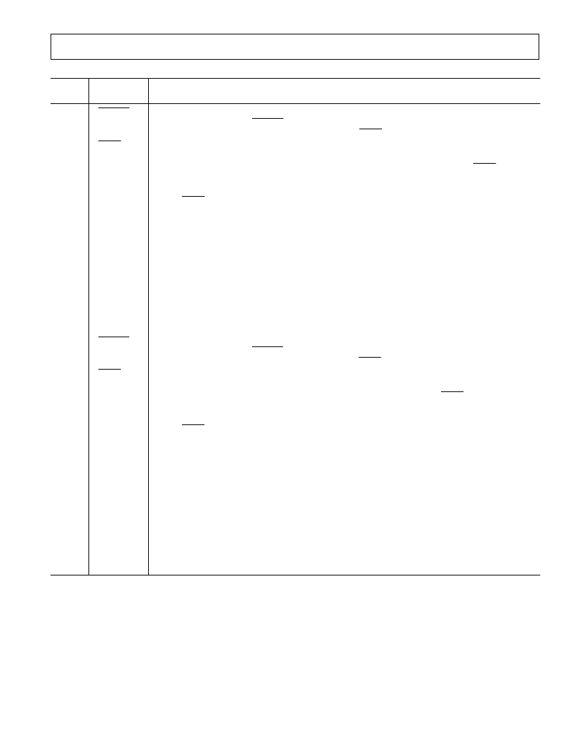
AD7242/AD7244 PIN FUNCTION DESCRIPTION
DIP
Pin No.
Mnemonic
Description
1
LDACA
Load DAC, Logic Input. A new word is transferred into DAC Latch A from input Latch A on the fall-
ing edge of this signal. If
LDACA
is hard-wired low, data is transferred from input Latch A to DAC
Latch A on the sixteenth falling edge of TCLKA after
TFSA
goes low.
Transmit Frame Synchronization, Logic Input. This is a frame or synchronization signal for DACA
data with serial data expected after the falling edge of this signal.
Transmit Data, Logic Input. This is the data input which is used in conjunction with
TFSA
and
TCLKA to transfer serial data to input Latch A.
Transmit Clock, Logic Input. Serial data bits for DACA are latched on the falling edge of TCLKA
when
TFSA
is low.
Digital Ground. Both DGND pins for the device must be tied together at the device.
Test Pin 1. Used when testing the device. Do not connect anything to this pin.
Positive Power Supply, 5 V
±
5%. Both V
DD
pins for the device must be tied together at the device.
Analog Ground. Both AGND pins for the device must be tied together at the device.
Analog Output Voltage from DACB. This output comes from a buffer amplifier. The range is bipolar,
±
3 V with REF INB = +3 V.
Negative Power Supply, –5 V
±
5%. Both V
SS
pins for the device must be tied together at the device.
Test Pin 2. Used when testing the device. Do not connect anything to this pin.
DACB Voltage Reference Input. The voltage reference for DACB is applied to this pin. It is internally
buffered before being applied to DACB. The nominal reference voltage for correct operation of the
AD7242/AD7244 is 3 V.
Load DAC, Logic Input. A new word is transferred into DAC Latch B from input Latch B on the fall-
ing edge of this signal. If
LDACB
is hard-wired low, data is transferred from input Latch B to DAC
Latch B on the sixteenth falling edge of TCLKB after
TFSB
goes low.
Transmit Frame Synchronization, Logic Input. This is a frame or synchronization signal for DACB
data with serial data expected after the falling edge of this signal.
Transmit Data, Logic Input. This is the data input used in conjunction with
TFSB
and TCLKB to
transfer serial data to input Latch B.
Transmit Clock, Logic Input. Serial data bits for DACB are latched on the falling edge of TCLKB
when
TFSB
is low.
Digital Ground. Both DGND pins for the device must be tied together at the device.
Test Pin 3. Used when testing the device. Do not connect anything to this pin.
Positive Power Supply, 5 V
±
5%. Both V
DD
pins for the device must be tied together at the device.
Analog Ground. Both AGND pins for the device must be tied together at the device.
Analog Output Voltage from DACA. This output comes from a buffer amplifier. The range is bipolar,
±
3 V with REF INA = +3 V.
Negative Power Supply, –5 V
±
5%. Both V
SS
pins for the device must be tied together at the device.
Voltage Reference Output. To operate the DACs with this internal reference, REF OUT should be
connected to both REF INA and REF INB. The external load capability of the reference is 500
μ
A.
DACA Voltage Reference Input. The voltage reference for DACA is applied to this pin. It is internally
buffered before being applied to DACA. The nominal reference voltage for correct operation of the
AD7242/AD7244 is 3 V.
2
TFSA
3
DTA
4
TCLKA
5
6
7
8
9
DGND
TP1
V
DD
AGND
V
OUTB
10
11
12
V
SS
TP2
REF INB
13
LDACB
14
TFSB
15
DTB
16
TCLKB
17
18
19
20
21
DGND
TP3
V
DD
AGND
V
OUTA
22
23
V
SS
REF OUT
24
REF INA
相关PDF资料 |
PDF描述 |
|---|---|
| AD7243 | LC2MOS 12-Bit Serial DACPORT |
| AD7243AN | LC2MOS 12-Bit Serial DACPORT |
| AD7243AQ | LC2MOS 12-Bit Serial DACPORT |
| AD7243AR | LC2MOS 12-Bit Serial DACPORT |
| AD7243BN | 47 UF, 20V CAP., TANTALUM |
相关代理商/技术参数 |
参数描述 |
|---|---|
| AD7242JR | 制造商:Analog Devices 功能描述: |
| AD7242KN | 制造商:AD 制造商全称:Analog Devices 功能描述:LC2MOS Dual, Complete, 12-Bit/14-Bit Serial DACs |
| AD7242KR | 制造商:AD 制造商全称:Analog Devices 功能描述:LC2MOS Dual, Complete, 12-Bit/14-Bit Serial DACs |
| AD7243 | 制造商:AD 制造商全称:Analog Devices 功能描述:LC2MOS 12-Bit Serial DACPORT |
| AD7243AN | 功能描述:IC SRL DAC 12BIT LC2MOS 16-DIP RoHS:否 类别:集成电路 (IC) >> 数据采集 - 数模转换器 系列:DACPORT® 产品培训模块:Data Converter Fundamentals DAC Architectures 标准包装:750 系列:- 设置时间:7µs 位数:16 数据接口:并联 转换器数目:1 电压电源:双 ± 功率耗散(最大):100mW 工作温度:0°C ~ 70°C 安装类型:表面贴装 封装/外壳:28-LCC(J 形引线) 供应商设备封装:28-PLCC(11.51x11.51) 包装:带卷 (TR) 输出数目和类型:1 电压,单极;1 电压,双极 采样率(每秒):143k |
发布紧急采购,3分钟左右您将得到回复。