参数资料
| 型号: | AD7244AQ |
| 厂商: | Analog Devices Inc |
| 文件页数: | 12/12页 |
| 文件大小: | 0K |
| 描述: | IC DAC 14BIT SRL W/REF 24-CDIP |
| 产品培训模块: | Data Converter Fundamentals DAC Architectures |
| 标准包装: | 1 |
| 设置时间: | 4µs |
| 位数: | 14 |
| 数据接口: | 串行 |
| 转换器数目: | 2 |
| 电压电源: | 双 ± |
| 功率耗散(最大): | 195mW |
| 工作温度: | -40°C ~ 85°C |
| 安装类型: | 通孔 |
| 封装/外壳: | 24-CDIP(0.300",7.62mm) |
| 供应商设备封装: | 24-CDIP |
| 包装: | 管件 |
| 输出数目和类型: | 2 电压,双极 |
| 采样率(每秒): | 250k |
AD7242/AD7244
REV. A
–9–
MICROPROCESSOR INTERFACING
Microprocessor interfacing to the AD7242/AD7244 is via a
serial bus that uses standard protocol compatible with DSP
processors and microcontrollers. The communication interface
consists of a separate transmit section for each of the DACs.
Each section has a clock signal, a data signal and a frame or
strobe pulse.
Figures 7 through 11 show the AD7242/AD7244 configured
for interfacing to a number of popular DSP processors and
microcontrollers.
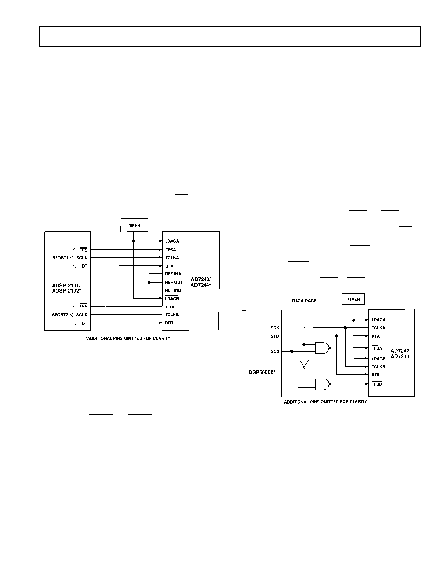
AD7242/AD7244 to ADSP-2101/ADSP-2102 Interface
Figure 7 shows a serial interface between the AD7242/AD7244
and the ADSP-2101/ADSP-2102 DSP processor. The ADSP-
2101/ADSP-2102 has two serial ports and, in the interface
shown, both serial ports are used, one for each DAC. Both serial
ports do not have to be used; in the case where only one serial
port is used, an extra line (DACA/DACB as shown in the other
serial interfaces) would have to decode the one TFS line to
provide TFSA and TFSB lines for the AD7242/AD7244.
Figure 7. AD7242/AD7244 to ADSP-2101/ADSP-2102
Interface
The three serial lines of the first serial port, SPORT1, of the
ADSP-2101/ADSP-2102 connect directly to the three serial
input lines of DACA of the AD7242/AD7244. The three serial
lines of SPORT2 connect directly to the three serial lines on the
DACB serial input port. Data from the ADSP-2101/ADSP-2102 is
valid on the falling edge of SCLK. A common LDAC signal is
used to drive the LDACA and LDACB inputs. This is shown to
be generated from a timer or clock recovery circuit but another
control or address line of the ADSP-2101/ADSP-2102 could be
used to drive these inputs. Alternatively, the LDACA and
LDACB
inputs of the AD7242/AD7244 could be hardwired
low; in this case the update of the DAC latches and analog
outputs takes place on the 16th falling edge of SCLK (after the
respective TFS signal goes low).
AD7242/AD7244 to DSP56000 Interface
A serial interface between the AD7242/AD7244 and the
DSP56000 is shown in Figure 8. The DSP56000 is configured
for normal mode, asynchronous operation with gated clock. It is
also set up for a 16-bit word with SCK and SC2 as outputs and
the FSL control bit set to a 0. SCK is internally generated on
the DSP56000 and applied to both the TCLKA and TCLKB
inputs of the AD7242/AD7244. Data from the DSP56000 is
valid on the falling edge of SCK. The serial data line, STD
drives the DTA and DTB serial input data lines of the
AD7242/AD7244.
The SC2 output provides the framing pulse for valid data. This
is an active high output and is gated with a DACA/DACB
control line before being applied to the TFSA and TFSB inputs
of the AD7242/AD7244. The DACA/DACB line determines
which DAC serial data is to be transferred to, i.e., which TFS
line is active when SC2 is active.
As in the previous interface, a common LDAC input is shown
driving the LDACA and LDACB inputs of the AD7242/AD7244.
Once again, these LDAC inputs could be hardwired low, in
which case VOUTA or VOUTB will be updated on the sixteenth
falling edge of SCK after the TFSA or TFSB input goes low.
Figure 8. AD7242/AD7244 to DSP56000 Interface
相关PDF资料 |
PDF描述 |
|---|---|
| AD7247AQ | IC DAC 12BIT W/AMP W/BUFF 24CDIP |
| AD7248AQ | IC DAC 12BIT W/REF 24-CDIP |
| AD7249BR | IC DAC 12BIT SRL W/REF 16-SOIC |
| AD7262BSTZ | IC ADC 2CH 12BIT PGA/COM 48LQFP |
| AD7264BCPZ | IC ADC 14BIT 2CH 1MSPS 48LFCSP |
相关代理商/技术参数 |
参数描述 |
|---|---|
| AD7244JN | 功能描述:IC DAC 14BIT SRL W/REF 24-DIP RoHS:否 类别:集成电路 (IC) >> 数据采集 - 数模转换器 系列:- 标准包装:2,400 系列:- 设置时间:- 位数:18 数据接口:串行 转换器数目:3 电压电源:模拟和数字 功率耗散(最大):- 工作温度:-40°C ~ 85°C 安装类型:表面贴装 封装/外壳:36-TFBGA 供应商设备封装:36-TFBGA 包装:带卷 (TR) 输出数目和类型:* 采样率(每秒):* |
| AD7244JNZ | 功能描述:IC DAC 14BIT SERIAL W/REF 24DIP RoHS:是 类别:集成电路 (IC) >> 数据采集 - 数模转换器 系列:- 标准包装:1 系列:- 设置时间:4.5µs 位数:12 数据接口:串行,SPI? 转换器数目:1 电压电源:单电源 功率耗散(最大):- 工作温度:-40°C ~ 125°C 安装类型:表面贴装 封装/外壳:8-SOIC(0.154",3.90mm 宽) 供应商设备封装:8-SOICN 包装:剪切带 (CT) 输出数目和类型:1 电压,单极;1 电压,双极 采样率(每秒):* 其它名称:MCP4921T-E/SNCTMCP4921T-E/SNRCTMCP4921T-E/SNRCT-ND |
| AD7244JR | 功能描述:IC DAC 14BIT LC2MOS DUAL 28SOIC RoHS:否 类别:集成电路 (IC) >> 数据采集 - 数模转换器 系列:- 产品培训模块:Lead (SnPb) Finish for COTS Obsolescence Mitigation Program 标准包装:1,000 系列:- 设置时间:1µs 位数:8 数据接口:串行 转换器数目:8 电压电源:双 ± 功率耗散(最大):941mW 工作温度:0°C ~ 70°C 安装类型:表面贴装 封装/外壳:24-SOIC(0.295",7.50mm 宽) 供应商设备封装:24-SOIC W 包装:带卷 (TR) 输出数目和类型:8 电压,单极 采样率(每秒):* |
| AD7244JR-REEL | 制造商:Rochester Electronics LLC 功能描述:- Tape and Reel |
| AD7244JRZ | 功能描述:IC DAC 14BIT LC2MOS DUAL 28SOIC RoHS:是 类别:集成电路 (IC) >> 数据采集 - 数模转换器 系列:- 标准包装:1 系列:- 设置时间:4.5µs 位数:12 数据接口:串行,SPI? 转换器数目:1 电压电源:单电源 功率耗散(最大):- 工作温度:-40°C ~ 125°C 安装类型:表面贴装 封装/外壳:8-SOIC(0.154",3.90mm 宽) 供应商设备封装:8-SOICN 包装:剪切带 (CT) 输出数目和类型:1 电压,单极;1 电压,双极 采样率(每秒):* 其它名称:MCP4921T-E/SNCTMCP4921T-E/SNRCTMCP4921T-E/SNRCT-ND |
发布紧急采购,3分钟左右您将得到回复。