参数资料
| 型号: | AD7248ABRZ |
| 厂商: | Analog Devices Inc |
| 文件页数: | 3/16页 |
| 文件大小: | 0K |
| 描述: | IC DAC 12BIT W/REF 20-SOIC |
| 产品培训模块: | Data Converter Fundamentals DAC Architectures |
| 标准包装: | 37 |
| 系列: | DACPORT® |
| 设置时间: | 7µs |
| 位数: | 12 |
| 数据接口: | 并联 |
| 转换器数目: | 1 |
| 电压电源: | 双 ± |
| 功率耗散(最大): | 210mW |
| 工作温度: | -40°C ~ 85°C |
| 安装类型: | 表面贴装 |
| 封装/外壳: | 20-SOIC(0.295",7.50mm 宽) |
| 供应商设备封装: | 20-SOIC W |
| 包装: | 管件 |
| 输出数目和类型: | 1 电压,单极;1 电压,双极 |
| 采样率(每秒): | 142k |
AD7245A/AD7248A
REV. B
–11–
BIPOLAR CONFIGURATION
The bipolar configuration for the AD7245A/AD7248A, which
gives an output voltage range from –5 V to +5 V, is achieved by
connecting the ROFS input to REF OUT and connecting RFB
and VOUT. The AD7245A/AD7248A must be operated from
dual supplies to achieve this output voltage range. The code
table for bipolar operation is shown in Table IV.
Table IV. Bipolar Code Table
DAC Latch Contents
MSB
LSB
Analog Output, VOUT
1 1 1 1
+VREF
×
2047
2048
1 0 0 0
0 0 0 0
0 0 0 1
+VREF
×
1
2048
1 0 0 0
0 0 0 0
0 V
0 1 1 1
1 1 1 1
–VREF
×
1
2048
0 0 0 0
0 0 0 1
–VREF
×
2047
2048
0 0 0 0
–VREF
×
2048
= –V
REF
NOTE:
1 LSB = 2
× V
REF(2
–11) = V
REF
1
2048
AGND BIAS
The AD7245A/AD7248A AGND pin can be biased above sys-
tem GND (AD7245A/AD7248A DGND) to provide an offset
“zero” analog output voltage level. With unity gain on the
amplifier (ROFS = VOUT = RFB) the output voltage, VOUT is
expressed as:
VOUT = VBIAS + D
VREF
where D is a fractional representation of the digital word in the
DAC latch and VBIAS is the voltage applied to the AD7245A/
AD7248A AGND pin.
Because the current flowing out of the AGND pin varies with
digital code, the AGND pin should be driven from a low imped-
ance source. A circuit configuration is outlined for AGND bias
in Figure 9 using the AD589, a +1.23 V bandgap reference.
If a gain of 2 is used on the buffer amplifier the output voltage,
VOUT is expressed as
VOUT = 2(VBIAS + D
VREF)
In this case care must be taken to ensure that the maximum
output voltage is not greater than VDD –3 V. The VDD–VOUT
overhead must be greater than 3 V to ensure correct operation
of the part. Note that VDD and VSS for the AD7245A/AD7248A
must be referenced to DGND (system GND). The entire circuit
can be operated in single supply with the VSS pin of the
AD7245A/AD7248A connected to system GND.
REF
DAC
AD7245A/AD7248A*
15V
0.1 F
10
+
10 F
ROFS
VDD
2R
RFB
VOUT
VSS
DGND
AD589
27k
AGND
VBIAS
REF OUT
VREF
SYSTEM
GND
*DIGITAL CIRCUITRY
OMITTED FOR CLARITY.
+
–
Figure 9. AGND Bias Circuit
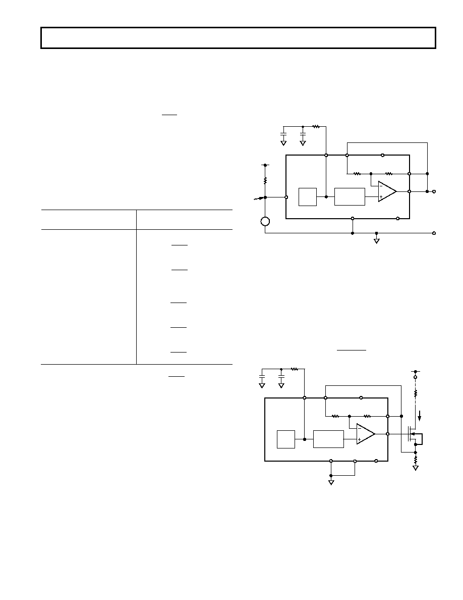
PROGRAMMABLE CURRENT SINK
Figure 10 shows how the AD7245A/AD7248A can be config-
ured with a power MOSFET transistor, the VN0300M, to
provide a programmable current sink from VDD or VSOURCE.
The VN0300M is placed in the feedback of the AD7245A/
AD7248A amplifier. The entire circuit can be operated in single
supply by tying the VSS of the AD7245A/AD7248A to AGND.
The sink current, ISINK, can be expressed as:
ISINK =
D
×V
REF
R1
REF
DAC
AD7245A/AD7248A*
0.1 F
10
+
10 F
ROFS
VDD
2R
RFB
VOUT
VSS
DGND
REF OUT
VREF
*DIGITAL CIRCUITRY
OMITTED FOR CLARITY.
AGND
VSOURCE
ISINK
LOAD
VN0300M
R1
Figure 10. Programmable Current Sink
Using the VN0300M, the voltage drop across the load can typi-
cally be as large as VSOURCE –6 V) with VOUT of the DAC at
5 V. Therefore, for a current of 50 mA flowing in the R1 (with
all 1s in the DAC register) the maximum load is 200
with
VSOURCE = 15 V. The VN0300M can actually handle currents
up to 500 mA and still function correctly in the circuit, but in
practice the circuit must be used with larger values of VSOURCE
otherwise it requires a very small load.
UNIPOLAR (0 V TO 5 V) CONFIGURATION
The 0 V to 5 V output voltage range is achieved by tying ROFS,
RFB and VOUT together. For this output range the AD7245A/
AD7248A can be operated single supply (VSS = 0 V) or dual sup-
ply. The table for output voltage versus digital code is as in Table
III, with 2
× V
REF replaced by VREF. Note that for this range
1 LSB = VREF(2
–12) = V
REF
1
4096
.
相关PDF资料 |
PDF描述 |
|---|---|
| AD7538JR | IC DAC 14BIT W/BUFF 24-SOIC |
| AD7548JPZ | IC DAC 12BIT MONO LC2MOS 20PLCC |
| DAC8043GPZ | IC DAC 12BIT MULTIPLY CMOS 8-DIP |
| AD7528LNZ | IC DAC 8BIT DUAL MULTIPLY 20-DIP |
| AD7225LR | IC DAC 8BIT QUAD W/AMP 24-SOIC |
相关代理商/技术参数 |
参数描述 |
|---|---|
| AD7248ABRZ-REEL | 功能描述:IC DAC 12BIT W/REF 20-SOIC RoHS:是 类别:集成电路 (IC) >> 数据采集 - 数模转换器 系列:DACPORT® 产品培训模块:Data Converter Fundamentals DAC Architectures 标准包装:750 系列:- 设置时间:7µs 位数:16 数据接口:并联 转换器数目:1 电压电源:双 ± 功率耗散(最大):100mW 工作温度:0°C ~ 70°C 安装类型:表面贴装 封装/外壳:28-LCC(J 形引线) 供应商设备封装:28-PLCC(11.51x11.51) 包装:带卷 (TR) 输出数目和类型:1 电压,单极;1 电压,双极 采样率(每秒):143k |
| AD7248AQ | 功能描述:IC DAC 12BIT W/REF 24-CDIP RoHS:否 类别:集成电路 (IC) >> 数据采集 - 数模转换器 系列:DACPORT® 产品培训模块:Data Converter Fundamentals DAC Architectures 标准包装:750 系列:- 设置时间:7µs 位数:16 数据接口:并联 转换器数目:1 电压电源:双 ± 功率耗散(最大):100mW 工作温度:0°C ~ 70°C 安装类型:表面贴装 封装/外壳:28-LCC(J 形引线) 供应商设备封装:28-PLCC(11.51x11.51) 包装:带卷 (TR) 输出数目和类型:1 电压,单极;1 电压,双极 采样率(每秒):143k |
| AD7248ASCHIPS | 功能描述:IC DAC 12BIT W/REF 制造商:analog devices inc. 系列:* 零件状态:上次购买时间 标准包装:1 |
| AD7248ASQ/883B | 制造商:未知厂家 制造商全称:未知厂家 功能描述:12-Bit Digital-to-Analog Converter |
| AD7248ATQ | 制造商:Analog Devices 功能描述:DAC 1CH R-2R 12-BIT 20CDIP - Rail/Tube 制造商:Rochester Electronics LLC 功能描述:12-BIT DACPORT (8+4) IC - Bulk 制造商:Analog Devices 功能描述:IC DAC 12BIT W/REF 24-CDIP 制造商:Analog Devices 功能描述:CONVERTER - DAC |
发布紧急采购,3分钟左右您将得到回复。