参数资料
| 型号: | AD7248ABRZ |
| 厂商: | Analog Devices Inc |
| 文件页数: | 6/16页 |
| 文件大小: | 0K |
| 描述: | IC DAC 12BIT W/REF 20-SOIC |
| 产品培训模块: | Data Converter Fundamentals DAC Architectures |
| 标准包装: | 37 |
| 系列: | DACPORT® |
| 设置时间: | 7µs |
| 位数: | 12 |
| 数据接口: | 并联 |
| 转换器数目: | 1 |
| 电压电源: | 双 ± |
| 功率耗散(最大): | 210mW |
| 工作温度: | -40°C ~ 85°C |
| 安装类型: | 表面贴装 |
| 封装/外壳: | 20-SOIC(0.295",7.50mm 宽) |
| 供应商设备封装: | 20-SOIC W |
| 包装: | 管件 |
| 输出数目和类型: | 1 电压,单极;1 电压,双极 |
| 采样率(每秒): | 142k |
AD7245A/AD7248A
REV. B
–14–
68008
AS
R/
W
D0–D7
ADDRESS
DECODE
ADDRESS BUS
*LINEAR CIRCUITRY OMITTED FOR CLARITY
DATA BUS
AD7248A*
CSLSB
LDAC
WR
DB0–DB7
DTACK
CSMSB
A0–A19
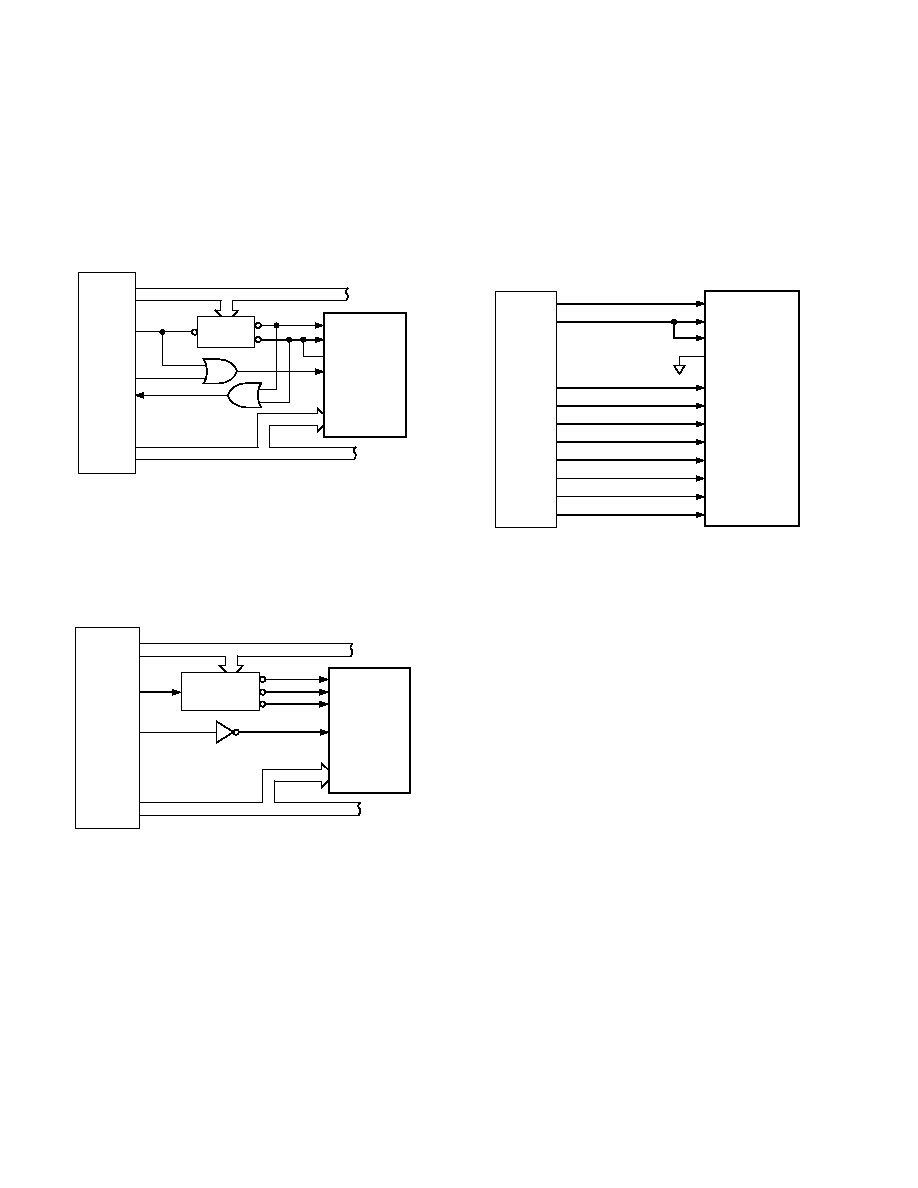
Figure 16. AD7248A to 68008 Interface
An interface circuit for connections to the 6502 or 6809 micro-
processors is shown in Figure 17. Once again, the AD7248A is
memory mapped and data is right justified. The procedure for
writing data to the AD7248A is as outlined for the 8085A/8088.
For the 6502 microprocessor the
φ2 clock is used to generate
the
WR, while for the 6809 the E signal is used.
6502/6809
R/
W
2 OR E
D0–D7
ADDRESS
DECODE
ADDRESS BUS
*LINEAR CIRCUITRY OMITTED FOR CLARITY.
DATA BUS
AD7248A*
CSLSB
LDAC
WR
DB0–DB7
CSMSB
A0–A15
EN
Figure 17. AD7248A to 6502/6809 Interface
Figure 18 shows a connection diagram between the AD7248A
and the 8051 microprocessor. The AD7248A is port mapped in
this interface and is configured in the automatic transfer mode.
Data to be loaded to the input latch low byte is output to Port 1.
Output Line P3.0, which is connected to
CSLSB of the AD7248A,
is pulsed to load data into the low byte of the input latch. Puls-
ing the P3.1 line, after the high byte data has been set up on
Port 1, updates the output of the AD7248A. The
WR input of the
AD7248A can be hardwired low in this application because
spurious address strobes on
CSLSB and CSMSB do not occur.
P3.0
P3.1
P1.0
P1.1
P1.2
P1.3
P1.4
P1.5
P1.6
P1.7
8051
CSLSB
CSMSB
LDAC
WR
DB0
DB1
DB2
DB3
DB4
DB5
DB6
DB7
AD7248A*
*ADDITIONAL PINS OMITTED FOR CLARITY.
Figure 18. AD7248A to MCS-51 Interface
A connection diagram for the interface between the AD7248A
and 68008 microprocessor is shown in Figure 16. Once again
the AD7248A acts as a memory mapped device and data is right
justified. In this case the AD7248A is configured in the auto-
matic transfer mode which means that the high byte of the input
latch has the same address as the DAC latch. Data is written to
the AD7248A by first writing data to the AD7248A low byte.
Writing data to the high byte of the input latch also transfers the
input latch contents to the DAC latch and updates the output.
相关PDF资料 |
PDF描述 |
|---|---|
| AD7538JR | IC DAC 14BIT W/BUFF 24-SOIC |
| AD7548JPZ | IC DAC 12BIT MONO LC2MOS 20PLCC |
| DAC8043GPZ | IC DAC 12BIT MULTIPLY CMOS 8-DIP |
| AD7528LNZ | IC DAC 8BIT DUAL MULTIPLY 20-DIP |
| AD7225LR | IC DAC 8BIT QUAD W/AMP 24-SOIC |
相关代理商/技术参数 |
参数描述 |
|---|---|
| AD7248ABRZ-REEL | 功能描述:IC DAC 12BIT W/REF 20-SOIC RoHS:是 类别:集成电路 (IC) >> 数据采集 - 数模转换器 系列:DACPORT® 产品培训模块:Data Converter Fundamentals DAC Architectures 标准包装:750 系列:- 设置时间:7µs 位数:16 数据接口:并联 转换器数目:1 电压电源:双 ± 功率耗散(最大):100mW 工作温度:0°C ~ 70°C 安装类型:表面贴装 封装/外壳:28-LCC(J 形引线) 供应商设备封装:28-PLCC(11.51x11.51) 包装:带卷 (TR) 输出数目和类型:1 电压,单极;1 电压,双极 采样率(每秒):143k |
| AD7248AQ | 功能描述:IC DAC 12BIT W/REF 24-CDIP RoHS:否 类别:集成电路 (IC) >> 数据采集 - 数模转换器 系列:DACPORT® 产品培训模块:Data Converter Fundamentals DAC Architectures 标准包装:750 系列:- 设置时间:7µs 位数:16 数据接口:并联 转换器数目:1 电压电源:双 ± 功率耗散(最大):100mW 工作温度:0°C ~ 70°C 安装类型:表面贴装 封装/外壳:28-LCC(J 形引线) 供应商设备封装:28-PLCC(11.51x11.51) 包装:带卷 (TR) 输出数目和类型:1 电压,单极;1 电压,双极 采样率(每秒):143k |
| AD7248ASCHIPS | 功能描述:IC DAC 12BIT W/REF 制造商:analog devices inc. 系列:* 零件状态:上次购买时间 标准包装:1 |
| AD7248ASQ/883B | 制造商:未知厂家 制造商全称:未知厂家 功能描述:12-Bit Digital-to-Analog Converter |
| AD7248ATQ | 制造商:Analog Devices 功能描述:DAC 1CH R-2R 12-BIT 20CDIP - Rail/Tube 制造商:Rochester Electronics LLC 功能描述:12-BIT DACPORT (8+4) IC - Bulk 制造商:Analog Devices 功能描述:IC DAC 12BIT W/REF 24-CDIP 制造商:Analog Devices 功能描述:CONVERTER - DAC |
发布紧急采购,3分钟左右您将得到回复。