参数资料
| 型号: | AD725ARZ-R7 |
| 厂商: | Analog Devices Inc |
| 文件页数: | 5/20页 |
| 文件大小: | 0K |
| 描述: | IC ENCODER RGB TO NTSC 16-SOIC |
| 标准包装: | 400 |
| 类型: | 视频编码器 |
| 应用: | RGB 至 NTSC/PAL |
| 电压 - 电源,数字: | 4.75 V ~ 5.25 V |
| 安装类型: | 表面贴装 |
| 封装/外壳: | 16-SOIC(0.295",7.50mm 宽) |
| 供应商设备封装: | 16-SOIC W |
| 包装: | 带卷 (TR) |
AD725
REV. 0
–13–
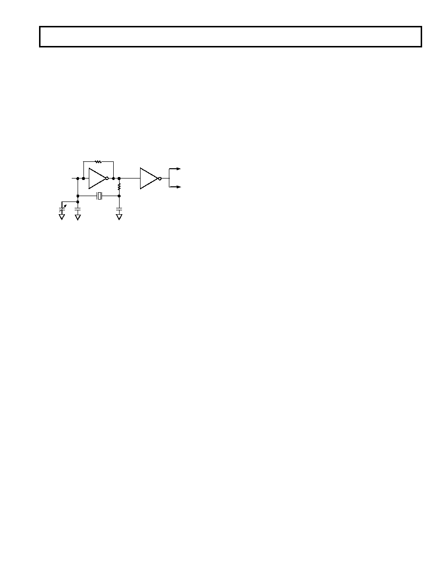
Low Cost Crystal Oscillator
A low cost oscillator can be made that provides a CW clock that
can be used to drive both the AD725 4FSC and other devices in
the system that require a clock at this frequency. Figure 20 shows a
circuit that uses one inverter of a 74HC04 package to create a
crystal oscillator and another inverter to buffer the oscillator
and drive other loads. The logic family must be a CMOS type
that can support the frequency of operation, and it must NOT
be a Schmitt trigger type of inverter. Resistor R1 from input to
output of U1A linearizes the inverter’s gain such that it provides
useful gain and a 180 degree phase shift to drive the oscillator.
R1
1M
Y1
TO PIN 3
OF AD725
U1A
U1B
R2
200
C2
60pF
C1
47pF
C3
~15pF
(OPT)
TO OTHER
DEVICE CLOCKS
HC04
Figure 20. Low Cost Crystal Oscillator
The crystal should be a parallel resonant type at the appropriate
frequency (NTSC/PAL, 4FSC). The series combination of C1
and C2 should approximately equal to the crystal manufacturer’s
specification for the parallel capacitance required for the crystal
to operate at its specified frequency. C1 will usually want to be
a somewhat smaller value because of the input parasitic capaci-
tance of the inverter. If it is desired to tune the frequency to
greater accuracy, C1 can be made still smaller and a parallel
adjustable capacitor can be used to adjust the frequency to the
desired accuracy.
Resistor R2 serves to provide the additional phase shift
required by the circuit to sustain oscillation. It can be sized by
R2 = 1/(2
× π × f × C2). Other functions of R2 are to provide a
low pass filter that suppresses oscillations at harmonics of the
fundamental of the crystal and to isolate the output of the in-
verter from the resonant load that the crystal network presents.
The basic oscillator described above is buffered by U1B to drive
the AD725 4FSC pin and other devices in the system. For a
system that requires both an NTSC and PAL oscillator, the
circuit can be duplicated by using a different pair of inverters
from the same package.
Dot Crawl
There are numerous distortions that are apparent in the presen-
tation of composite signals on TV monitors. These effects will
vary in degree depending on the circuitry used by the monitor
to process the signal and on the nature of the image being dis-
played. It is generally not possible to produce pictures on a
composite monitor that are as high quality as those produced by
standard quality RGB, VGA monitors.
One well known distortion of composite video images is called
dot crawl. It shows up as a moving dot pattern at the interface
between two areas of different color. It is caused by the inability
of the monitor circuitry to adequately separate the luminance
and chrominance signals.
One way to prevent dot crawl is to use a video signal that has
separate luminance and chrominance. Such a signal is referred
to as S-video or Y/C video. Since the luminance and chromi-
nance are already separated, the monitor does not have to per-
form this function. The S-video outputs of the AD725 can be
used to create higher quality pictures when there is an S-video
input available on the monitor.
Flicker
In a VGA conversion application, where the software controlled
registers are correctly set, there are two techniques that are
commonly used by VGA controller manufacturers to generate
the interlaced signal. Each of these techniques introduces a
unique characteristic into the display created by the AD725.
The artifacts described below are not due to the encoder or its
encoding algorithm as all encoders will generate the same dis-
play when presented with these inputs. They are due to the
method used by the controller display chip to convert a non-
interlaced output to an interlaced signal.
The first interlacing technique outputs a true interlaced signal
with odd and even fields (one each to a frame Figure 21a). This
provides the best picture quality when displaying photography,
CD video and animation (games, etc.). However, it will intro-
duce a defect commonly referred to as flicker into the display.
Flicker is a fundamental defect of all interlaced displays and is
caused by the alternating field characteristic of the interlace
technique. Consider a one pixel high black line which extends
horizontally across a white screen. This line will exist in only
one field and will be refreshed at a rate of 30 Hz (25 Hz for
PAL). During the time that the other field is being displayed the
line will not be displayed. The human eye is capable of detect-
ing this, and the display will be perceived to have a pulsating or
flickering black line. This effect is highly content sensitive and
is most pronounced in applications in which text and thin
horizontal lines are present. In applications such as CD video,
photography and animation, portions of objects naturally
occur in both odd and even fields and the effect of flicker is
imperceptible.
The second commonly used technique is to output an odd and
even field that are identical (Figure 21b). This ignores the data
that naturally occurs in one of the fields. In this case the same
one pixel high line mentioned above would either appear as a
two pixel high line, (one pixel high in both the odd and even field)
or not appear at all if it is in the data that is ignored by the control-
ler. Which of these cases occurs is dependent on the placement
of the line on the screen. This technique provides a stable (i.e.,
nonflickering) display for all applications, but small text can be
difficult to read and lines in drawings (or spreadsheets) can
disappear. As above, graphics and animation are not particularly
affected although some resolution is lost.
There are methods to dramatically reduce the effect of flicker and
maintain high resolution. The most common is to ensure that
display data never exists solely in a single line. This can be accom-
plished by averaging/weighting the contents of successive/multiple
noninterlaced lines prior to creating a true interlaced output (Fig-
ure 21c). In a sense, this provides an output that will lie between
the two extremes described above. The weight or percentage of
one line that appears in another, and the number of lines used,
are variables that must be considered in developing a system of
this type. If this type of signal processing is performed, it must
be completed prior to the data being presented to the AD725
for encoding.
相关PDF资料 |
PDF描述 |
|---|---|
| AD7294BCPZRL | IC ADC 12BIT I2C/SRL 1M 56LFCSP |
| AD7306AN | IC TXRX RS-232 RS-422 24-DIP |
| AD7339BSZ-REEL | IC ADC/QUAD DAC 5V W/REF 52-MQFP |
| AD7376ARUZ100 | IC POT DIGITAL 128POS 14-TSSOP |
| AD7391SRZ | IC DAC 10BIT SERIAL 3V 8SOIC |
相关代理商/技术参数 |
参数描述 |
|---|---|
| AD725ARZ-RL | 功能描述:IC ENCODER RGB TO NTSC 16-SOIC RoHS:是 类别:集成电路 (IC) >> 接口 - 编码器,解码器,转换器 系列:- 产品变化通告:Development Systems Discontinuation 26/Apr/2011 标准包装:1 系列:- 类型:编码器 应用:DVB-S.2 系统 电压 - 电源,模拟:- 电压 - 电源,数字:- 安装类型:- 封装/外壳:模块 供应商设备封装:模块 包装:散装 其它名称:Q4645799 |
| AD725ATQ | 制造商:Analog Devices 功能描述: |
| AD725EB | 制造商:Analog Devices 功能描述: |
| AD725-EB | 制造商:Analog Devices 功能描述:LOW COST RGB TO NTSC/PAL ENCODER W/ LUMA TRAP PORT - Bulk |
| AD725-EBZ | 制造商:Analog Devices 功能描述:EVALUATION BOARDS - Bulk |
发布紧急采购,3分钟左右您将得到回复。