参数资料
| 型号: | AD7262BSTZ |
| 厂商: | Analog Devices Inc |
| 文件页数: | 18/33页 |
| 文件大小: | 0K |
| 描述: | IC ADC 2CH 12BIT PGA/COM 48LQFP |
| 标准包装: | 1 |
| 位数: | 12 |
| 采样率(每秒): | 1M |
| 数据接口: | DSP,MICROWIRE?,QSPI?,串行,SPI? |
| 转换器数目: | 2 |
| 功率耗散(最大): | 120mW |
| 电压电源: | 单电源 |
| 工作温度: | -40°C ~ 105°C |
| 安装类型: | 表面贴装 |
| 封装/外壳: | 48-LQFP |
| 供应商设备封装: | 48-LQFP(7x7) |
| 包装: | 管件 |
| 输入数目和类型: | 2 个差分,单极 |
第1页第2页第3页第4页第5页第6页第7页第8页第9页第10页第11页第12页第13页第14页第15页第16页第17页当前第18页第19页第20页第21页第22页第23页第24页第25页第26页第27页第28页第29页第30页第31页第32页第33页
AD7262
Rev. 0 | Page 24 of 32
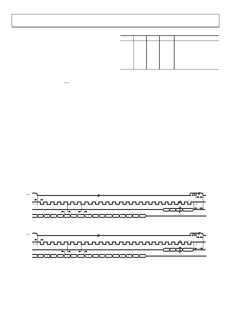
ON-CHIP REGISTERS
The AD7262/AD7262-5 contain a control register, two offset
registers for storing the offsets for each ADC, and two external
gain registers for storing the gain error. The control register and
the offset and gain registers are read and write registers. On
power-up, all registers in the AD7262/AD7262-5 are set to 0.
Addressing the On-Chip Registers
Writing to a Register
Data is loaded from the PD0/DIN pin of the AD7262/AD7262-5
on the falling edge of SCLK when CS is in a logic low state. Four
address bits and 12 data bits must be clocked into the device.
Thus, on the 16th falling SCLK edge, the LSB is clocked into the
AD7262/AD7262-5. One more SCLK cycle is then required to
write to the internal device registers. In total, 17 SCLK cycles
are required to successfully write to the AD7262/AD7262-5.
The control and offset registers are 12-bits registers; the gain
registers are 7-bit registers.
When writing to a register, the user must first write the address
bits corresponding to the selected register. Table 11 shows the
decoding of the address bits. The four RD bits are written MSB
first, that is, RD3 followed by RD2, RD1, and RD0. The
AD7262/AD7262-5 decodes these bits to determine which
register is being addressed. The subsequent 12 bits of data are
written to the addressed register.
When writing to the external gain registers, the seven bits of
data immediately after the four address bits are written to the
register. However, 17 SCLK cycles are still required, and the
PD0/DIN pin of the AD7262/AD7262-5 should be tied low for
the five additional clock cycles.
Table 11. Read and Write Register Addresses
RD3
RD2
RD1
RD0
Comment
0
ADC result (default)
0
1
Control register
0
1
0
Offset ADC A internal
0
1
Offset ADC B internal
0
1
0
Gain ADC A external
0
1
0
1
Gain ADC B external
Reading from a Register
The internal offset of the device, which has been measured by
the AD7262/AD7262-5 and stored in the on-chip registers
during the calibration, can be read back by the user. The
content of the external gain registers can also be read. To read
the content of any register, the user must first write to the
control register by writing 0001 to the WR3 to WR0 bits via the
control register are the RD bits, which are used to select the
desired register from which to read. The appropriate 4-bit address
for each of the offset and gain registers is outlined in Table 11.
The remaining eight SCLK cycles bits are used to set the
remaining bits in the control register to the desired state for the
next ADC conversion.
The 19th SCLK falling edge clocks out the first data bit of the
digital code corresponding to the value stored in the selected
internal device register on the DOUTA pin. DOUTB outputs the
conversion result from ADC B. Once the selected register has
been read, the control register must be reset to output the ADC
results for future conversions. This is achieved by writing 0001
to the WR3 to WR0 bits, followed by 0000 to the RD bits. The
remaining eight bits in the control register should then be set to
the required configuration for the next ADC conversion.
CS
SCLK
DOUTA
PD0/DIN
10
14
16
THREE-STATE
11
12
13
17
THREE-
STATE
15
DB10A
DB11A
DB0A
18
19
20
30
31
THREE-STATE
RD1
RD0
MSB DB10
DB9
DB8
DB7
DB6
DB5
DB4
DB3
DB2
DB1
DB0
RD2
RD3
t2
t8
t
QUIET
9
8
7
6
5
4
3
2
1
t13
t14
07
60
6-
0
31
Figure 31. Timing Diagram for Writing to a Register
CS
SCLK
DOUTA
PD0/DIN
10
14
16
THREE-STATE
11
12
13
17
THREE-
STATE
15
DB10A
DB11A
DB0A
18
20
19
30
31
THREE-STATE
0
1
RD3
RD2
RD1
RD0
0
t2
t13
t14
t8
tQUIET
9
8
7
6
5
4
3
2
1
07
60
6-
0
32
Figure 32. Timing Diagram for a Read Operation with PD0/DIN as an Input
相关PDF资料 |
PDF描述 |
|---|---|
| AD7264BCPZ | IC ADC 14BIT 2CH 1MSPS 48LFCSP |
| AD7265BSUZ-REEL7 | IC ADC 12BIT 3CHAN 1MSPS 32TQFP |
| AD7266BSUZ | IC ADC 12BIT 3CH 2MSPS 32-TQFP |
| AD7274BRM | IC ADC 12BIT 3MSPS HS LP 8MSOP |
| AD7276BRM | IC ADC 12BIT 3MSPS HS LP 8MSOP |
相关代理商/技术参数 |
参数描述 |
|---|---|
| AD7262BSTZ-5 | 功能描述:IC ADC 2CH 12BIT PGA/COM 48LQFP RoHS:是 类别:集成电路 (IC) >> 数据采集 - 模数转换器 系列:- 标准包装:1,000 系列:- 位数:16 采样率(每秒):45k 数据接口:串行 转换器数目:2 功率耗散(最大):315mW 电压电源:模拟和数字 工作温度:0°C ~ 70°C 安装类型:表面贴装 封装/外壳:28-SOIC(0.295",7.50mm 宽) 供应商设备封装:28-SOIC W 包装:带卷 (TR) 输入数目和类型:2 个单端,单极 |
| AD7262BSTZ-5-RL7 | 功能描述:IC ADC 12BIT W/PGA&COM 48-LQFP RoHS:是 类别:集成电路 (IC) >> 数据采集 - 模数转换器 系列:- 标准包装:1,000 系列:- 位数:16 采样率(每秒):45k 数据接口:串行 转换器数目:2 功率耗散(最大):315mW 电压电源:模拟和数字 工作温度:0°C ~ 70°C 安装类型:表面贴装 封装/外壳:28-SOIC(0.295",7.50mm 宽) 供应商设备封装:28-SOIC W 包装:带卷 (TR) 输入数目和类型:2 个单端,单极 |
| AD7262BSTZ-RL7 | 功能描述:IC ADC 12BIT W/PGA&COM 48-LQFP RoHS:是 类别:集成电路 (IC) >> 数据采集 - 模数转换器 系列:- 标准包装:1,000 系列:- 位数:16 采样率(每秒):45k 数据接口:串行 转换器数目:2 功率耗散(最大):315mW 电压电源:模拟和数字 工作温度:0°C ~ 70°C 安装类型:表面贴装 封装/外壳:28-SOIC(0.295",7.50mm 宽) 供应商设备封装:28-SOIC W 包装:带卷 (TR) 输入数目和类型:2 个单端,单极 |
| AD7264 | 制造商:AD 制造商全称:Analog Devices 功能描述:1 MSPS, 14-Bit, Simultaneous Sampling SAR ADC with PGA and Four Comparators |
| AD7264BCPZ | 功能描述:IC ADC 14BIT 2CH 1MSPS 48LFCSP RoHS:是 类别:集成电路 (IC) >> 数据采集 - 模数转换器 系列:- 标准包装:1,000 系列:- 位数:12 采样率(每秒):300k 数据接口:并联 转换器数目:1 功率耗散(最大):75mW 电压电源:单电源 工作温度:0°C ~ 70°C 安装类型:表面贴装 封装/外壳:24-SOIC(0.295",7.50mm 宽) 供应商设备封装:24-SOIC 包装:带卷 (TR) 输入数目和类型:1 个单端,单极;1 个单端,双极 |
发布紧急采购,3分钟左右您将得到回复。