- 您现在的位置:买卖IC网 > PDF目录10330 > AD7265BCPZ-REEL (Analog Devices Inc)IC ADC 12BIT 3CHAN 1MSPS 32LFCSP PDF资料下载
参数资料
| 型号: | AD7265BCPZ-REEL |
| 厂商: | Analog Devices Inc |
| 文件页数: | 16/29页 |
| 文件大小: | 0K |
| 描述: | IC ADC 12BIT 3CHAN 1MSPS 32LFCSP |
| 设计资源: | AD7265 in Differential and Single-Ended Configurations Using AD8022 (CN0048) |
| 标准包装: | 5,000 |
| 位数: | 12 |
| 采样率(每秒): | 1M |
| 数据接口: | DSP,MICROWIRE?,QSPI?,串行,SPI? |
| 转换器数目: | 2 |
| 功率耗散(最大): | 21mW |
| 电压电源: | 模拟和数字 |
| 工作温度: | -40°C ~ 125°C |
| 安装类型: | 表面贴装 |
| 封装/外壳: | 32-VFQFN 裸露焊盘,CSP |
| 供应商设备封装: | 32-LFCSP-VQ |
| 包装: | 带卷 (TR) |
| 输入数目和类型: | 12 个单端,单极;6 个差分,单极;6 个伪差分,单极 |
第1页第2页第3页第4页第5页第6页第7页第8页第9页第10页第11页第12页第13页第14页第15页当前第16页第17页第18页第19页第20页第21页第22页第23页第24页第25页第26页第27页第28页第29页
AD7265
Rev. A | Page 22 of 28
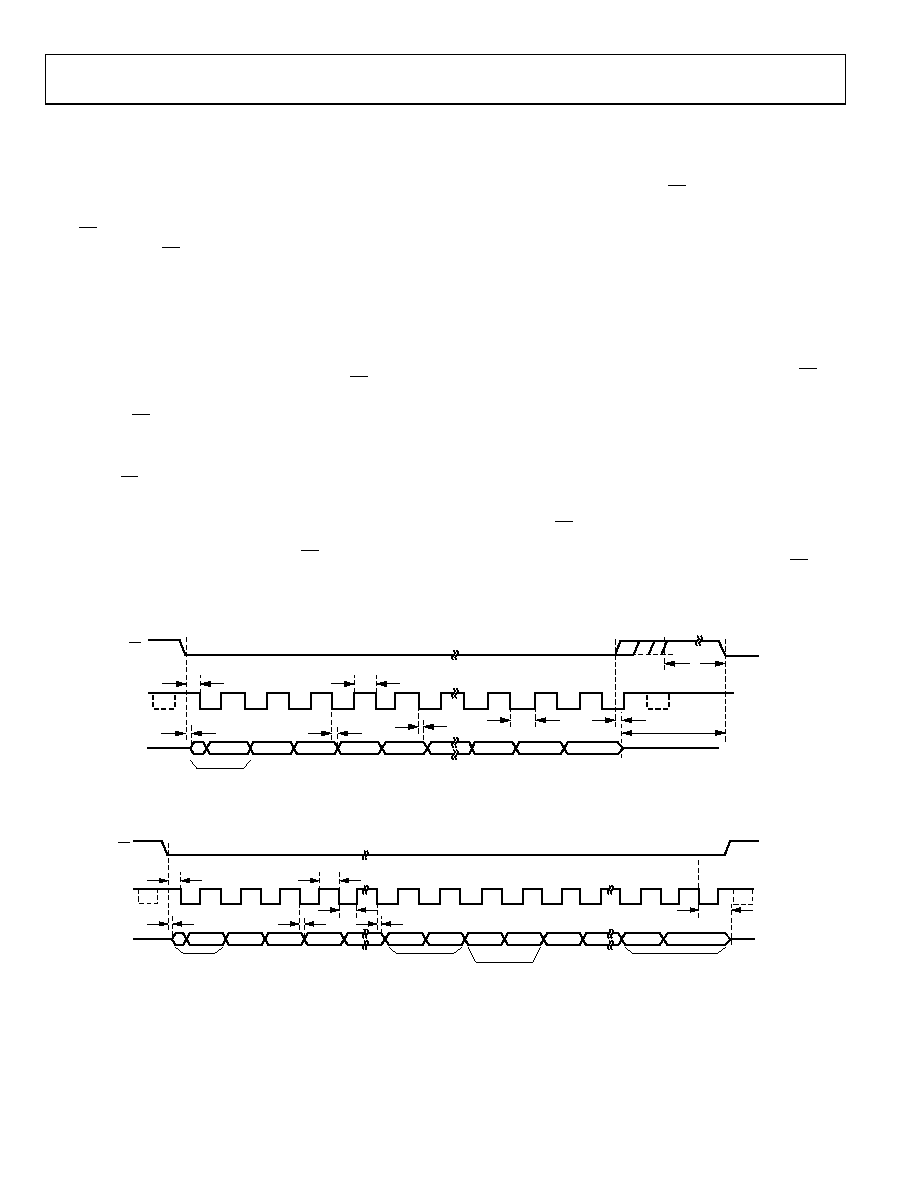
SERIAL INTERFACE
A minimum of 14 serial clock cycles are required to perform
the conversion process and to access data from one conversion
on either data line of the AD7265.
Figure 41 shows the detailed timing diagram for serial inter-
facing to the AD7265. The serial clock provides the conversion
clock and controls the transfer of information from the AD7265
during conversion.
CS going low provides the
leading zero to be read in by the microcontroller or DSP. The
remaining data is then clocked out by subsequent SCLK falling
edges, beginning with a second leading zero. Therefore, the first
falling clock edge on the serial clock has the leading zero pro-
vided and also clocks out the second leading zero. The 12-bit
result then follows with the final bit in the data transfer valid on
the 14
CS
The
signal initiates the data transfer and conversion process.
The falling edge of CS puts the track-and-hold into hold mode,
at which point the analog input is sampled and the bus is taken
out of three-state. The conversion is also initiated at this point
and requires a minimum of 14 SCLKs to complete. Once 13
SCLK falling edges have elapsed, the track-and-hold goes back
into track on the next SCLK rising edge, as shown in
th falling edge, having being clocked out on the previous
(13th) falling edge. It may also be possible to read in data on
each SCLK rising edge depending on the SCLK frequency or
the supply voltage. The first rising edge of SCLK after the
at Point B. If a 16-SCLK transfer is used, then two trailing zeros
will appear after the final LSB. On the rising edge of
CS
falling edge would have the second leading zero provided, and
the 13
CS, the
conversion is terminated and DOUTA and DOUTB go back into
three-state. If
th rising SCLK edge would have DB0 provided.
CS is not brought high but is instead held low for
a further 14 (or 16) SCLK cycles on D
Note that with fast SCLK values, and thus short SCLK periods,
in order to allow adequately for t
OUT
A, the data from Con-
version B is output on DOUTA (followed by 2 trailing zeros).
2
, an SCLK rising edge may
occur before the first SCLK falling edge. This rising edge of
SCLK can be ignored for the purposes of the timing descriptions in
this section. If a falling edge of SCLK is coincident with the
falling edge of
CS
Likewise, if
is held low for a further 14 (or 16) SCLK cycles
on D
B, the data from Conversion A is output on D
OUT
B. This
this case, the D
CS, then this falling edge of SCLK is not
acknowledged by the AD7265, and the next falling edge of
SCLK will be the first registered after the falling edge of
OUT
line in use goes back into three-state on the
32nd SCLK falling edge or the rising edge of CS, whichever
occurs first.
CS.
CS
SCLK
1
5
13
DOUTA
DOUTB
2 LEADING ZEROS
THREE-
STATE
t4
2
34
t5
t3
tQUIET
t2
THREE-STATE
DB11
DB10
DB2
DB0
t6
t7
t8
0
DB1
B
DB9
DB8
t9
04674-034
Figure 41. Serial Interface Timing Diagram
CS
SCLK
1
5
15
DOUTA
THREE-
STATE
t4
2
34
16
t5
t3
t2
THREE-
STATE
t6
t7
14
ZERO
0
ZERO
DB11B
17
2 LEADING ZEROS
t10
32
DB11A
2 LEADING
ZEROS
DB10A
DB9A
ZERO
2 TRAILING ZEROS
ZERO
2 TRAILING ZEROS
04674-035
Figure 42. Reading Data from Both ADCs on One D
Line with 32 SCLKs
OUT
相关PDF资料 |
PDF描述 |
|---|---|
| CS3106A-20-58P | CONN PLUG 10POS STRAIGHT W/PINS |
| AD7992BRMZ-0REEL | IC ADC 12BIT 2CHAN I2C 10MSOP |
| MS27468T17B99B | CONN HSG RCPT 23POS JAMNUT SCKT |
| MS3108A14S-2P | CONN PLUG 4POS RT ANG W/PINS |
| VE-24L-IU-S | CONVERTER MOD DC/DC 28V 200W |
相关代理商/技术参数 |
参数描述 |
|---|---|
| AD7265BCPZ-REEL7 | 功能描述:IC ADC 12BIT 3CHAN 1MSPS 32LFCSP RoHS:是 类别:集成电路 (IC) >> 数据采集 - 模数转换器 系列:- 标准包装:2,500 系列:- 位数:16 采样率(每秒):15 数据接口:MICROWIRE?,串行,SPI? 转换器数目:1 功率耗散(最大):480µW 电压电源:单电源 工作温度:-40°C ~ 85°C 安装类型:表面贴装 封装/外壳:38-WFQFN 裸露焊盘 供应商设备封装:38-QFN(5x7) 包装:带卷 (TR) 输入数目和类型:16 个单端,双极;8 个差分,双极 配用:DC1011A-C-ND - BOARD DELTA SIGMA ADC LTC2494 |
| AD7265BSU | 制造商:AD 制造商全称:Analog Devices 功能描述:Differential Input, Dual 1 MSPS, 12-Bit, 3-Channel SAR ADC |
| AD7265BSUZ | 功能描述:IC ADC 12BIT 3CHAN 1MSPS 32TQFP RoHS:是 类别:集成电路 (IC) >> 数据采集 - 模数转换器 系列:- 其它有关文件:TSA1204 View All Specifications 标准包装:1 系列:- 位数:12 采样率(每秒):20M 数据接口:并联 转换器数目:2 功率耗散(最大):155mW 电压电源:模拟和数字 工作温度:-40°C ~ 85°C 安装类型:表面贴装 封装/外壳:48-TQFP 供应商设备封装:48-TQFP(7x7) 包装:Digi-Reel® 输入数目和类型:4 个单端,单极;2 个差分,单极 产品目录页面:1156 (CN2011-ZH PDF) 其它名称:497-5435-6 |
| AD7265BSUZ-REEL | 功能描述:IC ADC 12BIT 3CHAN 1MSPS 32TQFP RoHS:是 类别:集成电路 (IC) >> 数据采集 - 模数转换器 系列:- 标准包装:2,500 系列:- 位数:16 采样率(每秒):15 数据接口:MICROWIRE?,串行,SPI? 转换器数目:1 功率耗散(最大):480µW 电压电源:单电源 工作温度:-40°C ~ 85°C 安装类型:表面贴装 封装/外壳:38-WFQFN 裸露焊盘 供应商设备封装:38-QFN(5x7) 包装:带卷 (TR) 输入数目和类型:16 个单端,双极;8 个差分,双极 配用:DC1011A-C-ND - BOARD DELTA SIGMA ADC LTC2494 |
| AD7265BSUZ-REEL7 | 功能描述:IC ADC 12BIT 3CHAN 1MSPS 32TQFP RoHS:是 类别:集成电路 (IC) >> 数据采集 - 模数转换器 系列:- 标准包装:1,000 系列:- 位数:16 采样率(每秒):45k 数据接口:串行 转换器数目:2 功率耗散(最大):315mW 电压电源:模拟和数字 工作温度:0°C ~ 70°C 安装类型:表面贴装 封装/外壳:28-SOIC(0.295",7.50mm 宽) 供应商设备封装:28-SOIC W 包装:带卷 (TR) 输入数目和类型:2 个单端,单极 |
发布紧急采购,3分钟左右您将得到回复。