- 您现在的位置:买卖IC网 > PDF目录10330 > AD7265BCPZ-REEL (Analog Devices Inc)IC ADC 12BIT 3CHAN 1MSPS 32LFCSP PDF资料下载
参数资料
| 型号: | AD7265BCPZ-REEL |
| 厂商: | Analog Devices Inc |
| 文件页数: | 6/29页 |
| 文件大小: | 0K |
| 描述: | IC ADC 12BIT 3CHAN 1MSPS 32LFCSP |
| 设计资源: | AD7265 in Differential and Single-Ended Configurations Using AD8022 (CN0048) |
| 标准包装: | 5,000 |
| 位数: | 12 |
| 采样率(每秒): | 1M |
| 数据接口: | DSP,MICROWIRE?,QSPI?,串行,SPI? |
| 转换器数目: | 2 |
| 功率耗散(最大): | 21mW |
| 电压电源: | 模拟和数字 |
| 工作温度: | -40°C ~ 125°C |
| 安装类型: | 表面贴装 |
| 封装/外壳: | 32-VFQFN 裸露焊盘,CSP |
| 供应商设备封装: | 32-LFCSP-VQ |
| 包装: | 带卷 (TR) |
| 输入数目和类型: | 12 个单端,单极;6 个差分,单极;6 个伪差分,单极 |
第1页第2页第3页第4页第5页当前第6页第7页第8页第9页第10页第11页第12页第13页第14页第15页第16页第17页第18页第19页第20页第21页第22页第23页第24页第25页第26页第27页第28页第29页
AD7265
Rev. A | Page 13 of 28
THEORY OF OPERATION
When the ADC starts a conversion (see Figure 17), SW3 opens
and SW1 and SW2 move to Position B, causing the comparator
to become unbalanced. Both inputs are disconnected once the
conversion begins. The control logic and the charge redistribution
DACs are used to add and subtract fixed amounts of charge
from the sampling capacitor arrays to bring the comparator
back into a balanced condition. When the comparator is
rebalanced, the conversion is complete. The control logic
generates the ADC output code. The output impedances of the
sources driving the V
CIRCUIT INFORMATION
The AD7265 is a fast, micropower, dual, 12-bit, single-supply,
ADC that operates from a 2.7 V to a 5.25 V supply. When
operated from either a 3 V or a 5 V supply, the AD7265 is
capable of throughput rates of 1 MSPS when provided with a
16 MHz clock.
The AD7265 contains two on-chip, differential track-and-hold
amplifiers, two successive approximation ADCs, and a serial
interface with two separate data output pins. It is housed in a
32-lead LFCSP or a 32-lead TQFP, offering the user
considerable space-saving advantages over alternative solutions.
The serial clock input accesses data from the part, but also
provides the clock source for each successive approximation
ADC. The analog input range for the part can be selected to be
a 0 V to V
and V
IN+
IN
pins must be matched;
otherwise, the two inputs will have different settling times,
resulting in errors.
CAPACITIVE
DAC
CAPACITIVE
DAC
CONTROL
LOGIC
COMPARATOR
SW3
SW1
A
B
SW2
CS
VIN+
VIN–
VREF
04674-014
input or a 2 × V
REF
input, configured with either
single-ended or differential analog inputs. The AD7265 has an
on-chip 2.5 V reference that can be overdriven when an external
reference is preferred. If the internal reference is to be used
elsewhere in a system, then the output needs to be buffered first.
The AD7265 also features power-down options to allow power
saving between conversions. The power-down feature is
implemented via the standard serial interface, as described in
the
Figure 17. ADC Conversion Phase
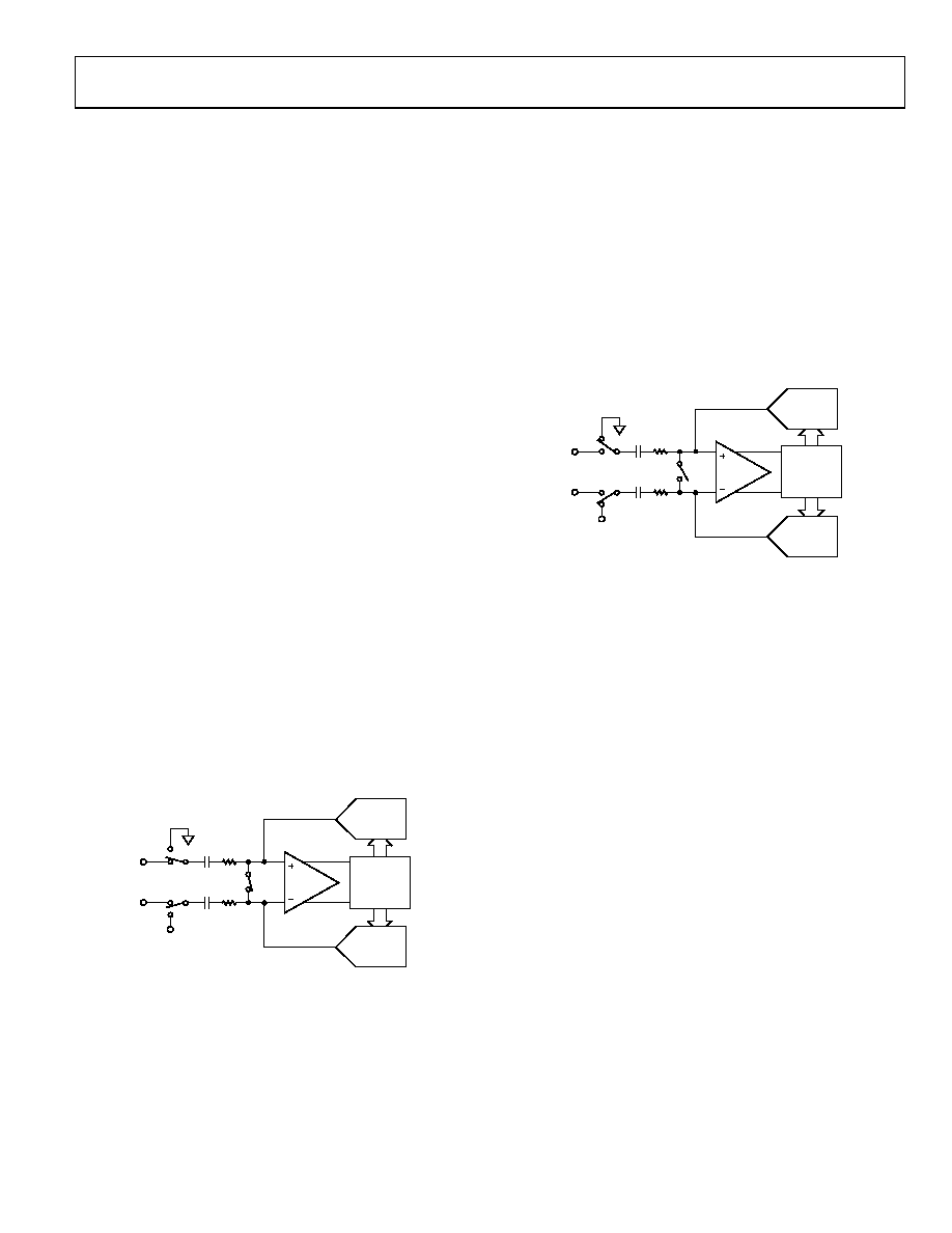
ANALOG INPUT STRUCTURE
Modes of Operation section.
Figure 18 shows the equivalent circuit of the analog input
structure of the AD7265 in differential/pseudo differential
modes. In single-ended mode, V
CONVERTER OPERATION
The AD7265 has two successive approximation ADCs, each
based around two capacitive DACs.
IN
is internally tied to AGND.
The four diodes provide ESD protection for the analog inputs.
Care must be taken to ensure that the analog input signals never
exceed the supply rails by more than 300 mV. This causes these
diodes to become forward-biased and starts conducting into the
substrate. These diodes can conduct up to 10 mA without
causing irreversible damage to the part.
show simplified schematics of one of these ADCs in acquisition
and conversion phase, respectively. The ADC is comprised of
control logic, a SAR, and two capacitive DACs. In Figure 16 (the
acquisition phase), SW3 is closed, SW1 and SW2 are in Position A,
the comparator is held in a balanced condition, and the sampling
capacitor arrays acquire the differential signal on the input.
The C1 capacitors in Figure 18 are typically 4 pF and can
primarily be attributed to pin capacitance. The resistors are
lumped components made up of the on resistance of the
switches. The value of these resistors is typically about 100 Ω.
The C2 capacitors are the ADC’s sampling capacitors with a
capacitance of 45 pF typically.
CAPACITIVE
DAC
CAPACITIVE
DAC
CONTROL
LOGIC
COMPARATOR
SW3
SW1
A
B
SW2
CS
VIN+
VIN–
VREF
04
67
4-
01
3
For ac applications, removing high frequency components from
the analog input signal is recommended by the use of an RC
low-pass filter on the relevant analog input pins with optimum
values of 47 Ω and 10 pF. In applications where harmonic
distortion and signal-to-noise ratio are critical, the analog input
should be driven from a low impedance source. Large source
impedances significantly affect the ac performance of the ADC
and may necessitate the use of an input buffer amplifier. The
choice of the op amp is a function of the particular application.
Figure 16. ADC Acquisition Phase
相关PDF资料 |
PDF描述 |
|---|---|
| CS3106A-20-58P | CONN PLUG 10POS STRAIGHT W/PINS |
| AD7992BRMZ-0REEL | IC ADC 12BIT 2CHAN I2C 10MSOP |
| MS27468T17B99B | CONN HSG RCPT 23POS JAMNUT SCKT |
| MS3108A14S-2P | CONN PLUG 4POS RT ANG W/PINS |
| VE-24L-IU-S | CONVERTER MOD DC/DC 28V 200W |
相关代理商/技术参数 |
参数描述 |
|---|---|
| AD7265BCPZ-REEL7 | 功能描述:IC ADC 12BIT 3CHAN 1MSPS 32LFCSP RoHS:是 类别:集成电路 (IC) >> 数据采集 - 模数转换器 系列:- 标准包装:2,500 系列:- 位数:16 采样率(每秒):15 数据接口:MICROWIRE?,串行,SPI? 转换器数目:1 功率耗散(最大):480µW 电压电源:单电源 工作温度:-40°C ~ 85°C 安装类型:表面贴装 封装/外壳:38-WFQFN 裸露焊盘 供应商设备封装:38-QFN(5x7) 包装:带卷 (TR) 输入数目和类型:16 个单端,双极;8 个差分,双极 配用:DC1011A-C-ND - BOARD DELTA SIGMA ADC LTC2494 |
| AD7265BSU | 制造商:AD 制造商全称:Analog Devices 功能描述:Differential Input, Dual 1 MSPS, 12-Bit, 3-Channel SAR ADC |
| AD7265BSUZ | 功能描述:IC ADC 12BIT 3CHAN 1MSPS 32TQFP RoHS:是 类别:集成电路 (IC) >> 数据采集 - 模数转换器 系列:- 其它有关文件:TSA1204 View All Specifications 标准包装:1 系列:- 位数:12 采样率(每秒):20M 数据接口:并联 转换器数目:2 功率耗散(最大):155mW 电压电源:模拟和数字 工作温度:-40°C ~ 85°C 安装类型:表面贴装 封装/外壳:48-TQFP 供应商设备封装:48-TQFP(7x7) 包装:Digi-Reel® 输入数目和类型:4 个单端,单极;2 个差分,单极 产品目录页面:1156 (CN2011-ZH PDF) 其它名称:497-5435-6 |
| AD7265BSUZ-REEL | 功能描述:IC ADC 12BIT 3CHAN 1MSPS 32TQFP RoHS:是 类别:集成电路 (IC) >> 数据采集 - 模数转换器 系列:- 标准包装:2,500 系列:- 位数:16 采样率(每秒):15 数据接口:MICROWIRE?,串行,SPI? 转换器数目:1 功率耗散(最大):480µW 电压电源:单电源 工作温度:-40°C ~ 85°C 安装类型:表面贴装 封装/外壳:38-WFQFN 裸露焊盘 供应商设备封装:38-QFN(5x7) 包装:带卷 (TR) 输入数目和类型:16 个单端,双极;8 个差分,双极 配用:DC1011A-C-ND - BOARD DELTA SIGMA ADC LTC2494 |
| AD7265BSUZ-REEL7 | 功能描述:IC ADC 12BIT 3CHAN 1MSPS 32TQFP RoHS:是 类别:集成电路 (IC) >> 数据采集 - 模数转换器 系列:- 标准包装:1,000 系列:- 位数:16 采样率(每秒):45k 数据接口:串行 转换器数目:2 功率耗散(最大):315mW 电压电源:模拟和数字 工作温度:0°C ~ 70°C 安装类型:表面贴装 封装/外壳:28-SOIC(0.295",7.50mm 宽) 供应商设备封装:28-SOIC W 包装:带卷 (TR) 输入数目和类型:2 个单端,单极 |
发布紧急采购,3分钟左右您将得到回复。