- 您现在的位置:买卖IC网 > PDF目录10545 > AD7265BSUZ (Analog Devices Inc)IC ADC 12BIT 3CHAN 1MSPS 32TQFP PDF资料下载
参数资料
| 型号: | AD7265BSUZ |
| 厂商: | Analog Devices Inc |
| 文件页数: | 26/29页 |
| 文件大小: | 0K |
| 描述: | IC ADC 12BIT 3CHAN 1MSPS 32TQFP |
| 设计资源: | AD7265 in Differential and Single-Ended Configurations Using AD8022 (CN0048) |
| 标准包装: | 1 |
| 位数: | 12 |
| 采样率(每秒): | 1M |
| 数据接口: | DSP,MICROWIRE?,QSPI?,串行,SPI? |
| 转换器数目: | 2 |
| 功率耗散(最大): | 21mW |
| 电压电源: | 模拟和数字 |
| 工作温度: | -40°C ~ 125°C |
| 安装类型: | 表面贴装 |
| 封装/外壳: | 32-TQFP |
| 供应商设备封装: | 32-TQFP(7x7) |
| 包装: | 托盘 |
| 输入数目和类型: | 12 个单端,单极;6 个差分,单极;6 个伪差分,单极 |
第1页第2页第3页第4页第5页第6页第7页第8页第9页第10页第11页第12页第13页第14页第15页第16页第17页第18页第19页第20页第21页第22页第23页第24页第25页当前第26页第27页第28页第29页
AD7265
Rev. A | Page 5 of 28
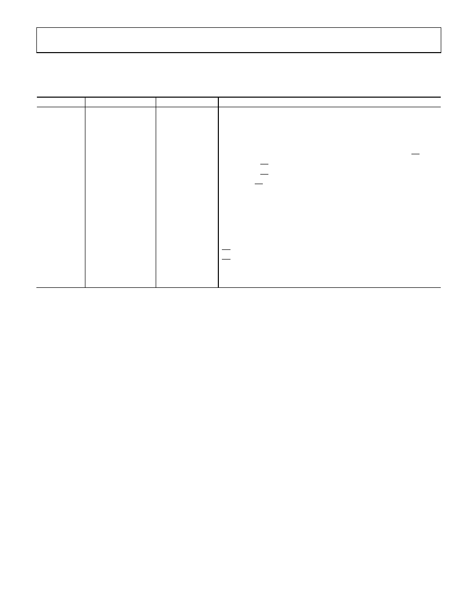
TIMING SPECIFICATIONS
AVDD = DVDD = 2.7 V to 5.25 V, VDRIVE = 2.7 V to 5.25 V, internal/external reference = 2.5 V, TA = TMAX to TMIN, unless otherwise noted1.
Table 2.
Parameter
Limit at TMIN, TMAX
Unit
Description
fSCLK2
1
MHz min
TA = 40°C to +85°C
4
MHz min
TA > 85°C to 125°C
16
MHz max
tCONVERT
14 × tSCLK
ns max
tSCLK = 1/fSCLK
875
ns max
fSCLK = 16 MHz
tQUIET
30
ns min
Minimum time between end of serial read and next falling edge of CS
t2
15/20
ns min
VDD = 5 V/3 V, CS to SCLK setup time, TA = 40°C to +85°C
20/30
ns min
VDD = 5 V/3 V, CS to SCLK setup time, TA > 85°C to 125°C
t3
15
ns max
Delay from CS until DOUTA and DOUTB are three-state disabled
t43
36
ns max
Data access time after SCLK falling edge, VDD = 3 V
27
ns max
Data access time after SCLK falling edge, VDD = 5 V
t5
0.45 tSCLK
ns min
SCLK low pulse width
t6
0.45 tSCLK
ns min
SCLK high pulse width
t7
10
ns min
SCLK to data valid hold time, VDD = 3 V
5
ns min
SCLK to data valid hold time, VDD = 5 V
t8
15
ns max
CS rising edge to DOUTA, DOUTB, high impedance
t9
30
ns min
CS rising edge to falling edge pulse width
t10
5
ns min
SCLK falling edge to DOUTA, DOUTB, high impedance
50
ns max
SCLK falling edge to DOUTA, DOUTB, high impedance
1 Sample tested during initial release to ensure compliance. All input signals are specified with tr = tf = 5 ns (10% to 90% of VDD) and timed from a voltage level of 1.6 V.
All timing specifications given are with a 25 pF load capacitance. With a load capacitance greater than this value, a digital buffer or latch must be used. See the Serial
2 Minimum SCLK for specified performance; with slower SCLK frequencies, performance specifications apply typically.
3 The time required for the output to cross 0.4 V or 2.4 V.
相关PDF资料 |
PDF描述 |
|---|---|
| VE-J13-MY-F2 | CONVERTER MOD DC/DC 24V 50W |
| IDT82P2282PFG | IC TXRX T1/J1/E1 2CH 100TQFP |
| IDT82P2281PFG | TXRX T1/E1/J1 LONG/SHORT 80-TQFP |
| VE-J12-MY-F2 | CONVERTER MOD DC/DC 15V 50W |
| LTC2498CUHF#PBF | IC ADC 24BIT 16CH 38-QFN |
相关代理商/技术参数 |
参数描述 |
|---|---|
| AD7265BSUZ-REEL | 功能描述:IC ADC 12BIT 3CHAN 1MSPS 32TQFP RoHS:是 类别:集成电路 (IC) >> 数据采集 - 模数转换器 系列:- 标准包装:2,500 系列:- 位数:16 采样率(每秒):15 数据接口:MICROWIRE?,串行,SPI? 转换器数目:1 功率耗散(最大):480µW 电压电源:单电源 工作温度:-40°C ~ 85°C 安装类型:表面贴装 封装/外壳:38-WFQFN 裸露焊盘 供应商设备封装:38-QFN(5x7) 包装:带卷 (TR) 输入数目和类型:16 个单端,双极;8 个差分,双极 配用:DC1011A-C-ND - BOARD DELTA SIGMA ADC LTC2494 |
| AD7265BSUZ-REEL7 | 功能描述:IC ADC 12BIT 3CHAN 1MSPS 32TQFP RoHS:是 类别:集成电路 (IC) >> 数据采集 - 模数转换器 系列:- 标准包装:1,000 系列:- 位数:16 采样率(每秒):45k 数据接口:串行 转换器数目:2 功率耗散(最大):315mW 电压电源:模拟和数字 工作温度:0°C ~ 70°C 安装类型:表面贴装 封装/外壳:28-SOIC(0.295",7.50mm 宽) 供应商设备封装:28-SOIC W 包装:带卷 (TR) 输入数目和类型:2 个单端,单极 |
| AD7266 | 制造商:Analog Devices 功能描述:- Bulk |
| AD7266ACP | 制造商:Analog Devices 功能描述:ADC DUAL SAR 2MSPS 12-BIT SERL 32LFCSP - Bulk |
| AD7266ASU | 制造商:Analog Devices 功能描述:ADC DUAL SAR 2MSPS 12-BIT SERL 32TQFP - Bulk |
发布紧急采购,3分钟左右您将得到回复。