参数资料
| 型号: | AD7274BRM |
| 厂商: | Analog Devices Inc |
| 文件页数: | 9/29页 |
| 文件大小: | 0K |
| 描述: | IC ADC 12BIT 3MSPS HS LP 8MSOP |
| 标准包装: | 50 |
| 位数: | 12 |
| 采样率(每秒): | 3M |
| 数据接口: | DSP,MICROWIRE?,QSPI?,串行,SPI? |
| 转换器数目: | 1 |
| 功率耗散(最大): | 18mW |
| 电压电源: | 单电源 |
| 工作温度: | -40°C ~ 125°C |
| 安装类型: | 表面贴装 |
| 封装/外壳: | 8-TSSOP,8-MSOP(0.118",3.00mm 宽) |
| 供应商设备封装: | 8-MSOP |
| 包装: | 管件 |
| 输入数目和类型: | 1 个单端,单极 |
第1页第2页第3页第4页第5页第6页第7页第8页当前第9页第10页第11页第12页第13页第14页第15页第16页第17页第18页第19页第20页第21页第22页第23页第24页第25页第26页第27页第28页第29页
AD7273/AD7274
Rev. 0 | Page 16 of 28
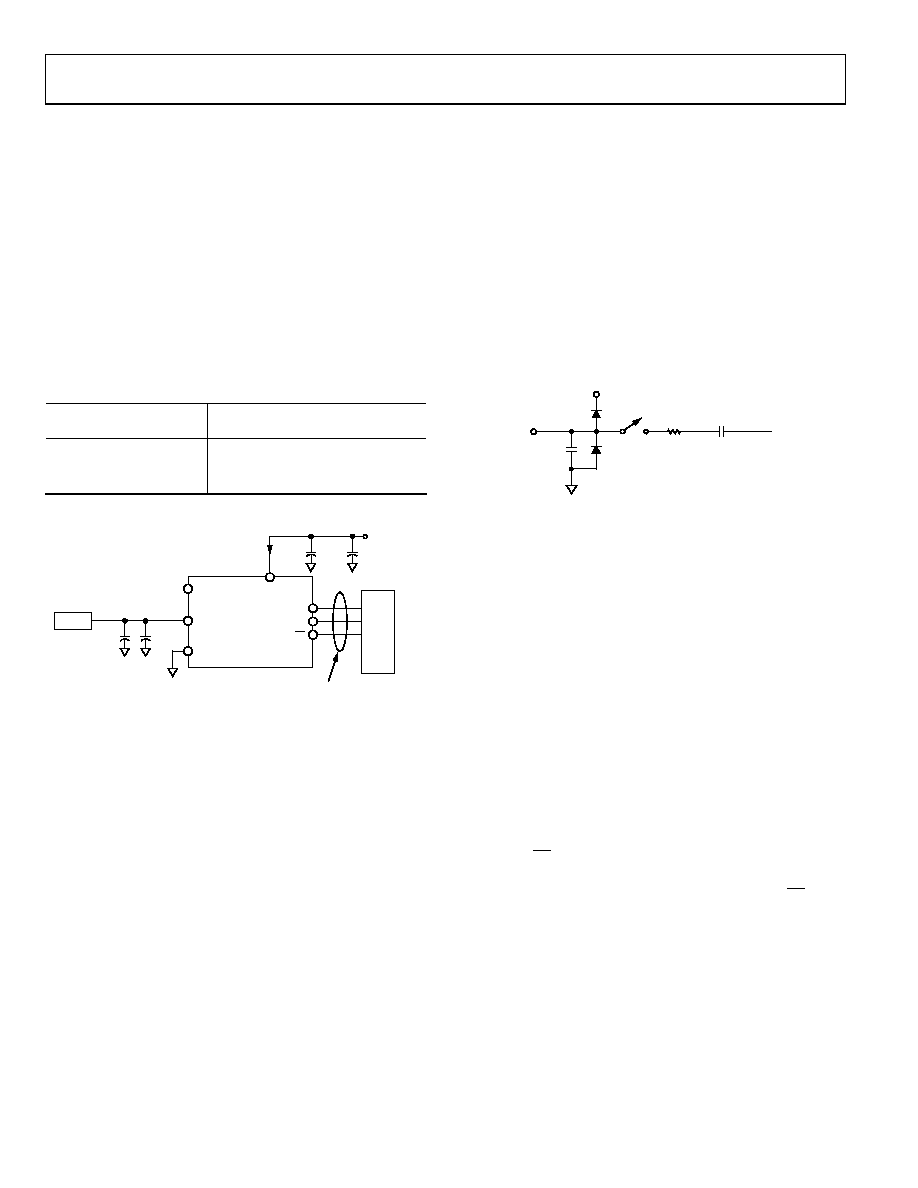
TYPICAL CONNECTION DIAGRAM
Figure 27 shows a typical connection diagram for the AD7273/
AD7274. An external reference must be applied to the ADC.
This reference can be in the range of 1.4 V to VDD. A precision
reference, such as the REF19x family or the ADR421, can be
used to supply the reference voltage to the AD7273/AD7274.
The conversion result is output in a 16-bit word with two leading
zeros followed by the 12-bit or 10-bit result. The 12-bit result from
the AD7274 is followed by two trailing zeros, and the 10-bit result
from the AD7273 is followed by four trailing zeros.
Table 7 provides some typical performance data with various
references under the same setup conditions for the AD7274.
Table 7. AD7274 Performance (Various Voltage Reference IC)
Voltage Reference
AD7274 SNR Performance
1 MHz Input
AD780 @ 2.5 V
71.3 dB
AD780 @ 3 V
70.1 dB
REF195
70.9 dB
AD7273/
AD7274
VDD
VIN
SERIAL
INTERFACE
0V TO VREF
INPUT
DSP/
μC/μP
VREF
AGND/DGND
SCLK
CS
SDATA
0.1
μF
10
μF
10pF
0.1
μF
2.5V
3.6V
SUPPLY
4.6 mA
REF195
04973-027
Figure 27. AD7273/AD7274 Typical Connection Diagram
ANALOG INPUT
Figure 28 shows an equivalent circuit of the analog input
structure of the AD7273/AD7274. The two diodes, D1 and D2,
provide ESD protection for the analog inputs. Care must be
taken to ensure that the analog input signal never exceeds the
supply rails by more than 300 mV. Signals exceeding this value
cause these diodes to become forward biased and to start
conducting current into the substrate. These diodes can
conduct a maximum current of 10 mA without causing
irreversible damage to the part. Capacitor C1 in Figure 28 is
typically about 4 pF and can primarily be attributed to pin
capacitance. Resistor R1 is a lumped component made up of the
on resistance of a switch. This resistor is typically about 75 Ω.
Capacitor C2 is the ADC sampling capacitor and has a capacitance
of 32 pF typically. For ac applications, removing high frequency
components from the analog input signal is recommended by
using a band-pass filter on the relevant analog input pin. In
applications where harmonic distortion and signal-to-noise
ratio are critical, the analog input should be driven from a low
impedance source. Large source impedances significantly affect
the ac performance of the ADCs. This may necessitate the use
of an input buffer amplifier. The AD8021 op amp is compatible
with this device; however, the choice of the op amp is a function
of the particular application.
C1
4pF
C2
R1
CONVERSION PHASE–SWITCH OPEN
TRACK PHASE–SWITCH CLOSED
D1
D2
VDD
VIN
04973-028
Figure 28. Equivalent Analog Input Circuit
When no amplifier is used to drive the analog input, the source
impedance should be limited to a low value. The maximum source
impedance depends on the amount of THD that can be tolerated.
The THD increases as the source impedance increases and perfor-
mance degrades. Figure 14 shows a graph of the THD vs. the
analog input frequency for different source impedances when
using a supply voltage of 3 V and sampling at a rate of 3 MSPS.
DIGITAL INPUTS
The digital inputs applied to the AD7273/AD7274 are not
limited by the maximum ratings that limit the analog inputs.
Instead, the digital inputs can be applied at up to 6 V and are
not restricted by the VDD + 0.3 V limit of the analog inputs. For
example, if the AD7273/AD7274 were operated with a VDD of
3 V, then 5 V logic levels could be used on the digital inputs.
However, it is important to note that the data output on SDATA
still has 3 V logic levels when VDD = 3 V. Another advantage of
SCLK and CS not being restricted by the VDD + 0.3 V limit is
that power supply sequencing issues are avoided. For example,
unlike with the analog inputs, with the digital inputs, if CS or
SCLK are applied before VDD, there is no risk of latch-up.
相关PDF资料 |
PDF描述 |
|---|---|
| AD7276BRM | IC ADC 12BIT 3MSPS HS LP 8MSOP |
| AD7291BCPZ-RL7 | IC ADC I2C/SRL 22.22K 20LFCSP |
| AD7298-1BCPZ-RL | IC ADC 10BIT SPI/SRL 8CH 20LFCSP |
| AD7298BCPZ-RL7 | IC ADC 10BIT SPI/SRL 8CH 20LFCSP |
| AD7302BRUZ-REEL7 | IC DAC 8BIT DUAL R-R 20-TSSOP |
相关代理商/技术参数 |
参数描述 |
|---|---|
| AD7274BRM-U2 | 制造商:Analog Devices 功能描述:ADC SGL SAR 3MSPS 12-BIT SERL 8MSOP - Bulk |
| AD7274BRMZ | 功能描述:IC ADC 12BIT 3MSPS HS LP 8MSOP RoHS:是 类别:集成电路 (IC) >> 数据采集 - 模数转换器 系列:- 标准包装:1,000 系列:- 位数:12 采样率(每秒):300k 数据接口:并联 转换器数目:1 功率耗散(最大):75mW 电压电源:单电源 工作温度:0°C ~ 70°C 安装类型:表面贴装 封装/外壳:24-SOIC(0.295",7.50mm 宽) 供应商设备封装:24-SOIC 包装:带卷 (TR) 输入数目和类型:1 个单端,单极;1 个单端,双极 |
| AD7274BRMZ2 | 制造商:AD 制造商全称:Analog Devices 功能描述:3 MSPS,10-/12-Bit ADCs in 8-Lead TSOT |
| AD7274BRMZ-REEL | 功能描述:IC ADC 12BIT 3MSPS HS LP 8MSOP RoHS:是 类别:集成电路 (IC) >> 数据采集 - 模数转换器 系列:- 标准包装:1,000 系列:- 位数:16 采样率(每秒):45k 数据接口:串行 转换器数目:2 功率耗散(最大):315mW 电压电源:模拟和数字 工作温度:0°C ~ 70°C 安装类型:表面贴装 封装/外壳:28-SOIC(0.295",7.50mm 宽) 供应商设备封装:28-SOIC W 包装:带卷 (TR) 输入数目和类型:2 个单端,单极 |
| AD7274BRMZ-REEL2 | 制造商:AD 制造商全称:Analog Devices 功能描述:3 MSPS,10-/12-Bit ADCs in 8-Lead TSOT |
发布紧急采购,3分钟左右您将得到回复。