- 您现在的位置:买卖IC网 > PDF目录10681 > AD7291BCPZ (Analog Devices Inc)IC ADC 12BIT SAR 8CH 20-LFCSP PDF资料下载
参数资料
| 型号: | AD7291BCPZ |
| 厂商: | Analog Devices Inc |
| 文件页数: | 5/29页 |
| 文件大小: | 0K |
| 描述: | IC ADC 12BIT SAR 8CH 20-LFCSP |
| 标准包装: | 1 |
| 位数: | 12 |
| 采样率(每秒): | 22.22k |
| 数据接口: | I²C,串行 |
| 转换器数目: | 1 |
| 功率耗散(最大): | 12.6mW |
| 电压电源: | 单电源 |
| 工作温度: | -40°C ~ 125°C |
| 安装类型: | 表面贴装 |
| 封装/外壳: | 20-WFQFN 裸露焊盘,CSP |
| 供应商设备封装: | 20-LFCSP-WQ(4x4) |
| 包装: | 托盘 |
| 输入数目和类型: | 8 个单端,单极 |
| 配用: | EVAL-AD7291SDZ-ND - BOARD EVAL FOR AD7291 |
第1页第2页第3页第4页当前第5页第6页第7页第8页第9页第10页第11页第12页第13页第14页第15页第16页第17页第18页第19页第20页第21页第22页第23页第24页第25页第26页第27页第28页第29页
AD7291
Data Sheet
Rev. B | Page 12 of 28
CIRCUIT INFORMATION
The AD7291 includes an 8-channel multiplexer, an on-chip
track-and-hold amplifier, an analog-to-digital converter (ADC),
an on-chip oscillator, internal data registers, an internal tempera-
ture sensor, and an I2C-compatible serial interface, all housed in
a 20-lead LFCSP. This package offers considerable space-saving
advantages over alternative solutions. The part can be operated
from a single supply from 2.8 V to 3.6 V and offers 12 bits of
resolution. The AD7291 has eight single-ended input channels
and an on-chip ±12 ppm reference. The analog input range for
the AD7921 is 0 V to VREF. The AD7291 includes a high
accuracy band gap temperature sensor, which is monitored and
digitized by the 12-bit ADC to give a resolution of 0.25°C.
The AD7291 typically remains in a partial power-down state
while not converting. When supplies are first applied, the part
powers up in a partial power-down state. Power-up is initiated
prior to a conversion, and the device returns to partial power-
down mode when the conversion is complete. Conversions can
be initiated by using the autocycle mode or command mode
where wake-up and a conversion occur during a write address
function. When the conversion is complete, the AD7291 again
enters partial power-down mode.
In command mode at the beginning of a read, the AD7291
wakes up completely, that is, becomes fully functional and
completes the conversion while the address is being read out. In
autocylce mode, conversions occur at 50 μs intervals; that is, the
AD7291 exits partial power-down mode and powers up fully at
50 μs intervals. This automatic partial power-down feature
allows power saving between conversions. Any read or write
operation across the I2C interface can occur while the device is
in partial power-down mode.
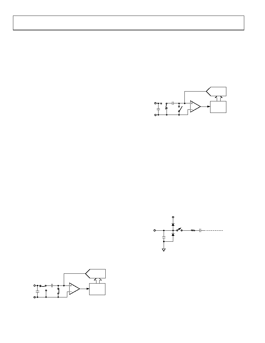
CONVERTER OPERATION
The AD7291 is a 12-bit successive approximation ADC based
fied schematics of the ADC during the acquisition and conversion
phase, respectively. The ADC comprises control logic, SAR,
and a capacitive DAC that are used to add and subtract fixed
amounts of charge from the sampling capacitor to bring the
comparator back into a balanced condition. Figure 18 shows the
acquisition phase. SW2 is closed and SW1 is in Position A, the
comparator is held in a balanced condition, and the sampling
capacitor acquires the signal on the selected VIN channel.
CONTROL
LOGIC
CAPACITIVE
DAC
VIN
A
B
SW1
SW2
GND1
COMPARATOR
08
71
1-
00
4
Figure 18. ADC Acquisition Phase
When the ADC starts a conversion (see Figure 19), SW2
opens and SW1 moves to Position B, causing the comparator
to become unbalanced. The control logic and the capacitive
DAC are used to add and subtract fixed amounts of charge to
bring the comparator back into a balanced condition. When the
comparator is rebalanced, the conversion is complete. The
control logic generates the ADC output code. Figure 21 shows
the transfer functions of the ADC.
CONTROL
LOGIC
CAPACITIVE
DACE
VIN
A
B
SW1
SW2
GND1
COMPARATOR
08
71
1-
00
5
Figure 19. ADC Conversion Phase
ANALOG INPUT
Figure 20 shows an equivalent circuit of the analog input struc-
ture of the AD7291. The two diodes, D1 and D2, provide ESD
protection for the analog inputs. Care must be taken to ensure
that the analog input signal never exceeds the internally generated
LDO voltage of 2.5 V (DCAP) by more than 300 mV. This causes
the diodes to become forward biased and start conducting
current into the substrate. The maximum current these diodes
can conduct without causing irreversible damage to the part is
10 mA. Capacitor C1, in Figure 20, is typically about 8 pF and
can primarily be attributed to pin capacitance. Resistor R1 is a
lumped component made up of the on resistance of a switch
(track-and-hold switch) and the on resistance of the input
multiplexer. The total resistance is typically about 155 Ω.
Capacitor C2 is the ADC sampling capacitor and has a
capacitance of 34 pF typically.
C1
8pF
C2
34pF
R1
D2
CONVERSION PHASE: SWITCH OPEN
TRACK PHASE: SWITCH CLOSED
D1
DCAP (2.5V)
VIN
0871
1-006
Figure 20. Equivalent Analog Input Circuit
For ac applications, removing high frequency components
from the analog input signal is recommended by using an RC
low-pass filter on the relevant analog input pin. In applications
where harmonic distortion and signal-to-noise ratios are
critical, the analog input should be driven from a low imped-
ance source. Large source impedances significantly affect the
ac performance of the ADC. This may necessitate the use of
an input buffer amplifier. The choice of the op amp is a function
of the particular application performance criteria.
相关PDF资料 |
PDF描述 |
|---|---|
| VI-26R-MY-B1 | CONVERTER MOD DC/DC 7.5V 50W |
| 1676850-1 | CAP CER 0.47PF 25V 5% NP0 0402 |
| VI-26L-MY-B1 | CONVERTER MOD DC/DC 28V 50W |
| VE-JWD-MY-F4 | CONVERTER MOD DC/DC 85V 50W |
| VI-24Y-MX-B1 | CONVERTER MOD DC/DC 3.3V 49.5W |
相关代理商/技术参数 |
参数描述 |
|---|---|
| AD7291BCPZ-RL7 | 功能描述:IC ADC I2C/SRL 22.22K 20LFCSP RoHS:是 类别:集成电路 (IC) >> 数据采集 - 模数转换器 系列:- 标准包装:1,000 系列:- 位数:16 采样率(每秒):45k 数据接口:串行 转换器数目:2 功率耗散(最大):315mW 电压电源:模拟和数字 工作温度:0°C ~ 70°C 安装类型:表面贴装 封装/外壳:28-SOIC(0.295",7.50mm 宽) 供应商设备封装:28-SOIC W 包装:带卷 (TR) 输入数目和类型:2 个单端,单极 |
| AD7291TCPZ-EP | 功能描述:CH 12 BIT SAR WT INTERNAL TEMP S 制造商:analog devices inc. 系列:- 包装:托盘 零件状态:在售 位数:12 采样率(每秒):22.22k 输入数:8 输入类型:单端 数据接口:I2C 配置:MUX-S/H-ADC 无线电 - S/H:ADC:1:1 A/D 转换器数:1 架构:SAR 参考类型:外部, 内部 电压 - 电源,模拟:2.8 V ~ 3.6 V 电压 - 电源,数字:2.8 V ~ 3.6 V 特性:温度传感器 工作温度:-55°C ~ 125°C(TA) 封装/外壳:20-WFQFN 裸露焊盘,CSP 供应商器件封装:20-LFCSP(4x4) 标准包装:1 |
| AD7291TCPZ-EP-RL7 | 功能描述:8 CH 12 BIT SAR WT INTERNAL TEMP 制造商:analog devices inc. 系列:- 包装:带卷(TR) 零件状态:在售 位数:12 采样率(每秒):22.22k 输入数:8 输入类型:单端 数据接口:I2C 配置:MUX-S/H-ADC 无线电 - S/H:ADC:1:1 A/D 转换器数:1 架构:SAR 参考类型:外部, 内部 电压 - 电源,模拟:2.8 V ~ 3.6 V 电压 - 电源,数字:2.8 V ~ 3.6 V 特性:温度传感器 工作温度:-55°C ~ 125°C(TA) 封装/外壳:20-WFQFN 裸露焊盘,CSP 供应商器件封装:20-LFCSP(4x4) 标准包装:1,500 |
| AD7292BCPZ | 制造商:Analog Devices 功能描述:Monitor and Control System 36-Pin LFCSP EP Tray 制造商:Analog Devices 功能描述:12-BIT,MULTI-CHANNEL, ADC,DAC WT TEMP IC - Trays 制造商:Analog Devices 功能描述:IC ADC 10BIT SPI/SRL 36-LFCSP 制造商:Analog Devices 功能描述:ADC DAC TEMP SENSOR GPIO 3 制造商:Analog Devices 功能描述:ADC, DAC, TEMP SENSOR, GPIO, 36LFCSP 制造商:Analog Devices Inc. 功能描述:Analog to Digital Converters - ADC 12-Bit Multi-Channel ADC DAC wt Temp IC 制造商:Analog Devices 功能描述:ANALOGUE MONITORING & CONTROL CIRCUIT, LFCSP-36; IC Function:Analogue Monitoring and Control Circuit; Supply Voltage Min:1.8V; Supply Voltage Max:5.25V; Operating Temperature Min:-40C; Operating Temperature Max:125C; No. of Pins:36;RoHS Compliant: Yes |
| AD7292BCPZ-RL | 制造商:Analog Devices 功能描述:Monitor and Control System 36-Pin LFCSP EP T/R 制造商:Analog Devices 功能描述:12-BIT,MULTI-CHANNEL, ADC,DAC WT TEMP IC - Tape and Reel 制造商:Analog Devices 功能描述:IC ADC 10BIT SPI/SRL 36LFCSP 制造商:Analog Devices Inc. 功能描述:Analog to Digital Converters - ADC 12-Bit Multi-Channel ADC DAC wt Temp IC 制造商:Analog Devices Inc. 功能描述:Analog to Digital Converters - ADC 10B Monitor & Cntrl System w/ Temp Sensr |
发布紧急采购,3分钟左右您将得到回复。