参数资料
| 型号: | AD7302BNZ |
| 厂商: | Analog Devices Inc |
| 文件页数: | 12/16页 |
| 文件大小: | 0K |
| 描述: | IC DAC 8BIT DUAL R-R 20-DIP |
| 产品培训模块: | Data Converter Fundamentals DAC Architectures |
| 标准包装: | 18 |
| 设置时间: | 1.2µs |
| 位数: | 8 |
| 数据接口: | 并联 |
| 转换器数目: | 2 |
| 电压电源: | 单电源 |
| 功率耗散(最大): | 24.8mW |
| 工作温度: | -40°C ~ 105°C |
| 安装类型: | 通孔 |
| 封装/外壳: | 20-DIP(0.300",7.62mm) |
| 供应商设备封装: | 20-PDIP |
| 包装: | 管件 |
| 输出数目和类型: | 2 电压,单极;2 电压,双极 |
| 采样率(每秒): | 833k |
| 产品目录页面: | 784 (CN2011-ZH PDF) |
AD7302
–5–
REV. 0
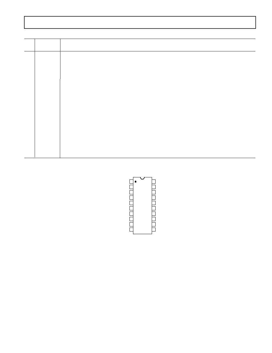
PIN FUNCTION DESCRIPTIONS
Pin
No.
Mnemonic Function
1-8
D7–D0
Parallel Data Inputs. Eight-bit data is loaded to the input register of the AD7302 under the control of
CS
and
WR.
9
CS
Chip Select. Active low logic input.
10
WR
Write Input.
WR is an active low logic input used in conjunction with CS and A/B to write data to the selected
DAC register.
11
A/B
DAC Select. Address pin used to select writing to either DAC A or DAC B.
12
PD
Active low input used to put the part into low power mode reducing current consumption to less than 1
A.
13
LDAC
Load DAC Logic Input. When this logic input is taken low both DAC outputs are simultaneously updated with
the contents of their DAC registers. If
LDAC is permanently tied low, the DACs are updated on the rising
edge of
WR.
14
CLR
Asynchronous Clear Input (Active Low). When this input is taken low the DAC registers are loaded with all
zeroes and the DAC outputs are cleared to zero volts.
15
VDD
Power Supply Input. These parts can be operated from 2.7 V to 5.5 V and should be decoupled to AGND.
16
REFIN
External Reference Input. This can used as the reference for both DACs. The range on this reference input is
1 V to VDD/2. If REFIN is directly tied to VDD the internal VDD/2 reference is selected.
17
AGND
Analog Ground reference point and return point for all analog current on the part.
18
VOUTB
Analog output voltage from DAC B. The output amplifier can swing rail to rail on its output.
19
VOUTA
Analog output voltage from DAC A. The output amplifier can swing rail to rail on its output.
20
DGND
Digital Ground reference point and return point for all digital current on the part.
PIN CONFIGURATION
14
13
12
11
17
16
15
20
19
18
10
9
8
1
2
3
4
7
6
5
TOP VIEW
(Not to Scale)
AD7302
(MSB) DB7
AGND
VOUTB
VOUTA
DGND
DB6
DB5
DB4
CLR
VDD
REFIN
DB3
DB2
DB1
(LSB) DB0
CS
WR
A/B
PD
LDAC
相关PDF资料 |
PDF描述 |
|---|---|
| AD5623RBRMZ-3 | IC DAC NANO 12BIT DUAL 10-MSOP |
| VE-BNX-MV-F1 | CONVERTER MOD DC/DC 5.2V 150W |
| VI-201-MY-F2 | CONVERTER MOD DC/DC 12V 50W |
| AD5623RBRMZ-5 | IC DAC NANO 12BIT DUAL 10-MSOP |
| MS3454W14S-7PW | CONN RCPT 3POS JAM NUT W/PINS |
相关代理商/技术参数 |
参数描述 |
|---|---|
| AD7302BR | 功能描述:IC DAC 8BIT DUAL 2.7V 20-SOIC RoHS:否 类别:集成电路 (IC) >> 数据采集 - 数模转换器 系列:- 标准包装:2,400 系列:- 设置时间:- 位数:18 数据接口:串行 转换器数目:3 电压电源:模拟和数字 功率耗散(最大):- 工作温度:-40°C ~ 85°C 安装类型:表面贴装 封装/外壳:36-TFBGA 供应商设备封装:36-TFBGA 包装:带卷 (TR) 输出数目和类型:* 采样率(每秒):* |
| AD7302BR-REEL | 制造商:Analog Devices 功能描述:DAC 2-CH 8-bit 20-Pin SOIC W T/R 制造商:Rochester Electronics LLC 功能描述:3V/5V DUAL 8-BIT DAC I.C. - Tape and Reel |
| AD7302BR-REEL7 | 功能描述:IC DAC 8BIT DUAL R-R 20-SOIC RoHS:否 类别:集成电路 (IC) >> 数据采集 - 数模转换器 系列:- 产品培训模块:Lead (SnPb) Finish for COTS Obsolescence Mitigation Program 标准包装:50 系列:- 设置时间:4µs 位数:12 数据接口:串行 转换器数目:2 电压电源:单电源 功率耗散(最大):- 工作温度:-40°C ~ 85°C 安装类型:表面贴装 封装/外壳:8-TSSOP,8-MSOP(0.118",3.00mm 宽) 供应商设备封装:8-uMAX 包装:管件 输出数目和类型:2 电压,单极 采样率(每秒):* 产品目录页面:1398 (CN2011-ZH PDF) |
| AD7302BRU | 功能描述:IC DAC 8BIT DUAL R-R 20-TSSOP RoHS:否 类别:集成电路 (IC) >> 数据采集 - 数模转换器 系列:- 标准包装:2,400 系列:- 设置时间:- 位数:18 数据接口:串行 转换器数目:3 电压电源:模拟和数字 功率耗散(最大):- 工作温度:-40°C ~ 85°C 安装类型:表面贴装 封装/外壳:36-TFBGA 供应商设备封装:36-TFBGA 包装:带卷 (TR) 输出数目和类型:* 采样率(每秒):* |
| AD7302BRU-REEL | 制造商:Analog Devices 功能描述:DAC 2-CH 8-bit 20-Pin TSSOP T/R 制造商:Analog Devices 功能描述:DAC 2CH 8BIT 20TSSOP - Tape and Reel |
发布紧急采购,3分钟左右您将得到回复。