参数资料
| 型号: | AD7302BNZ |
| 厂商: | Analog Devices Inc |
| 文件页数: | 3/16页 |
| 文件大小: | 0K |
| 描述: | IC DAC 8BIT DUAL R-R 20-DIP |
| 产品培训模块: | Data Converter Fundamentals DAC Architectures |
| 标准包装: | 18 |
| 设置时间: | 1.2µs |
| 位数: | 8 |
| 数据接口: | 并联 |
| 转换器数目: | 2 |
| 电压电源: | 单电源 |
| 功率耗散(最大): | 24.8mW |
| 工作温度: | -40°C ~ 105°C |
| 安装类型: | 通孔 |
| 封装/外壳: | 20-DIP(0.300",7.62mm) |
| 供应商设备封装: | 20-PDIP |
| 包装: | 管件 |
| 输出数目和类型: | 2 电压,单极;2 电压,双极 |
| 采样率(每秒): | 833k |
| 产品目录页面: | 784 (CN2011-ZH PDF) |
AD7302
–11–
REV. 0
VREF
is the voltage applied to the external REFIN pin when
the external reference is selected and is VDD/2 if the
internal reference is used.
Table I. Output Voltage for Selected Input Codes
Digital Input
MSB . . . LSB
Analog Output
1111 1111
2
× 255/256 × V
REF V
1111 1110
2
× 254/256 × V
REF V
1000 0001
2
× 129/256 × V
REF V
1000 0000
VREF V
0111 1111
2
× 127/256 × V
REF V
0000 0001
2
× V
REF/256 V
0000 0000
0 V
00
01
DAC INPUT
CODE
FF
80
81
FE
7F
0
2.VREF
VREF
DAC
OUTPUT
VOLTAGE
Figure 26. DAC Transfer Function
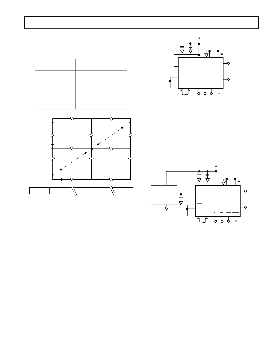
Figure 27 shows a typical setup for the AD7302 when using its
internal reference. The internal reference is selected by tying the
REFIN pin to VDD. Internally in the reference section there is a
reference detect circuit that will select the internal VDD/2 based
on the voltage connected to the REFIN pin. If REFIN is within
a threshold voltage of a PMOS device (approximately 1 V) of
VDD the internal reference is selected. When the REFIN voltage
is more than 1 V below VDD, the externally applied voltage at
this pin is used as the reference for the DAC. The internal
reference on the AD7302 is VDD/2, the output current to voltage
converter within the AD7302 provides a gain of two. Thus the
output range of the DAC is from 0 V to VDD, based on Table I.
AD7302
VOUTA
VOUTB
10F
0.1F
VDD = 3 TO 5V
VDD
A/B
REF IN
CLR
PD
VDD
AGND DGND
CS
WR LDAC
D7–D0
VOUTA
VOUTB
DATA BUS
CONTROL INPUTS
Figure 27. Typical Configuration Selecting the Internal
Reference
Figure 28 shows a typical setup for the AD7302 when using an
external reference. The reference range for the AD7302 is from
1 V to VDD/2 V. Higher values of reference can be incorporated,
but will saturate the output at both the top and bottom end of
the transfer function. There is a gain of two from input to output
on the AD7302. Suitable references for 5 V operation are the
AD780 and REF192. For 3 V operation a suitable external
reference would be the AD589 a 1.23 V bandgap reference.
AD7302
VOUTA
VOUTB
10F
0.1F
VDD = 3 TO 5V
VDD
AD780/REF192
WITH VDD = 5V
OR
AD589 WITH VDD = 3V
REF IN
GND
VOUT
VIN
0.1F
EXT REF
VDD
AGND DGND
D7–D0
VOUTA
VOUTB
DATA BUS
CONTROL INPUTS
A/B
CLR
PD
CS
WR LDAC
Figure 28. Typical Configuration Using An External
Reference
相关PDF资料 |
PDF描述 |
|---|---|
| AD5623RBRMZ-3 | IC DAC NANO 12BIT DUAL 10-MSOP |
| VE-BNX-MV-F1 | CONVERTER MOD DC/DC 5.2V 150W |
| VI-201-MY-F2 | CONVERTER MOD DC/DC 12V 50W |
| AD5623RBRMZ-5 | IC DAC NANO 12BIT DUAL 10-MSOP |
| MS3454W14S-7PW | CONN RCPT 3POS JAM NUT W/PINS |
相关代理商/技术参数 |
参数描述 |
|---|---|
| AD7302BR | 功能描述:IC DAC 8BIT DUAL 2.7V 20-SOIC RoHS:否 类别:集成电路 (IC) >> 数据采集 - 数模转换器 系列:- 标准包装:2,400 系列:- 设置时间:- 位数:18 数据接口:串行 转换器数目:3 电压电源:模拟和数字 功率耗散(最大):- 工作温度:-40°C ~ 85°C 安装类型:表面贴装 封装/外壳:36-TFBGA 供应商设备封装:36-TFBGA 包装:带卷 (TR) 输出数目和类型:* 采样率(每秒):* |
| AD7302BR-REEL | 制造商:Analog Devices 功能描述:DAC 2-CH 8-bit 20-Pin SOIC W T/R 制造商:Rochester Electronics LLC 功能描述:3V/5V DUAL 8-BIT DAC I.C. - Tape and Reel |
| AD7302BR-REEL7 | 功能描述:IC DAC 8BIT DUAL R-R 20-SOIC RoHS:否 类别:集成电路 (IC) >> 数据采集 - 数模转换器 系列:- 产品培训模块:Lead (SnPb) Finish for COTS Obsolescence Mitigation Program 标准包装:50 系列:- 设置时间:4µs 位数:12 数据接口:串行 转换器数目:2 电压电源:单电源 功率耗散(最大):- 工作温度:-40°C ~ 85°C 安装类型:表面贴装 封装/外壳:8-TSSOP,8-MSOP(0.118",3.00mm 宽) 供应商设备封装:8-uMAX 包装:管件 输出数目和类型:2 电压,单极 采样率(每秒):* 产品目录页面:1398 (CN2011-ZH PDF) |
| AD7302BRU | 功能描述:IC DAC 8BIT DUAL R-R 20-TSSOP RoHS:否 类别:集成电路 (IC) >> 数据采集 - 数模转换器 系列:- 标准包装:2,400 系列:- 设置时间:- 位数:18 数据接口:串行 转换器数目:3 电压电源:模拟和数字 功率耗散(最大):- 工作温度:-40°C ~ 85°C 安装类型:表面贴装 封装/外壳:36-TFBGA 供应商设备封装:36-TFBGA 包装:带卷 (TR) 输出数目和类型:* 采样率(每秒):* |
| AD7302BRU-REEL | 制造商:Analog Devices 功能描述:DAC 2-CH 8-bit 20-Pin TSSOP T/R 制造商:Analog Devices 功能描述:DAC 2CH 8BIT 20TSSOP - Tape and Reel |
发布紧急采购,3分钟左右您将得到回复。