- 您现在的位置:买卖IC网 > PDF目录165342 > AD7302BNZ (ANALOG DEVICES INC) 2.7 V to 5.5 V, Parallel Input Dual Voltage Output 8-Bit DAC PDF资料下载
参数资料
| 型号: | AD7302BNZ |
| 厂商: | ANALOG DEVICES INC |
| 元件分类: | DAC |
| 英文描述: | 2.7 V to 5.5 V, Parallel Input Dual Voltage Output 8-Bit DAC |
| 中文描述: | PARALLEL, 8 BITS INPUT LOADING, 1.2 us SETTLING TIME, 8-BIT DAC, PDIP20 |
| 封装: | PLASTIC, DIP-20 |
| 文件页数: | 2/16页 |
| 文件大小: | 292K |
| 代理商: | AD7302BNZ |
AD7302
–10–
REV. 0
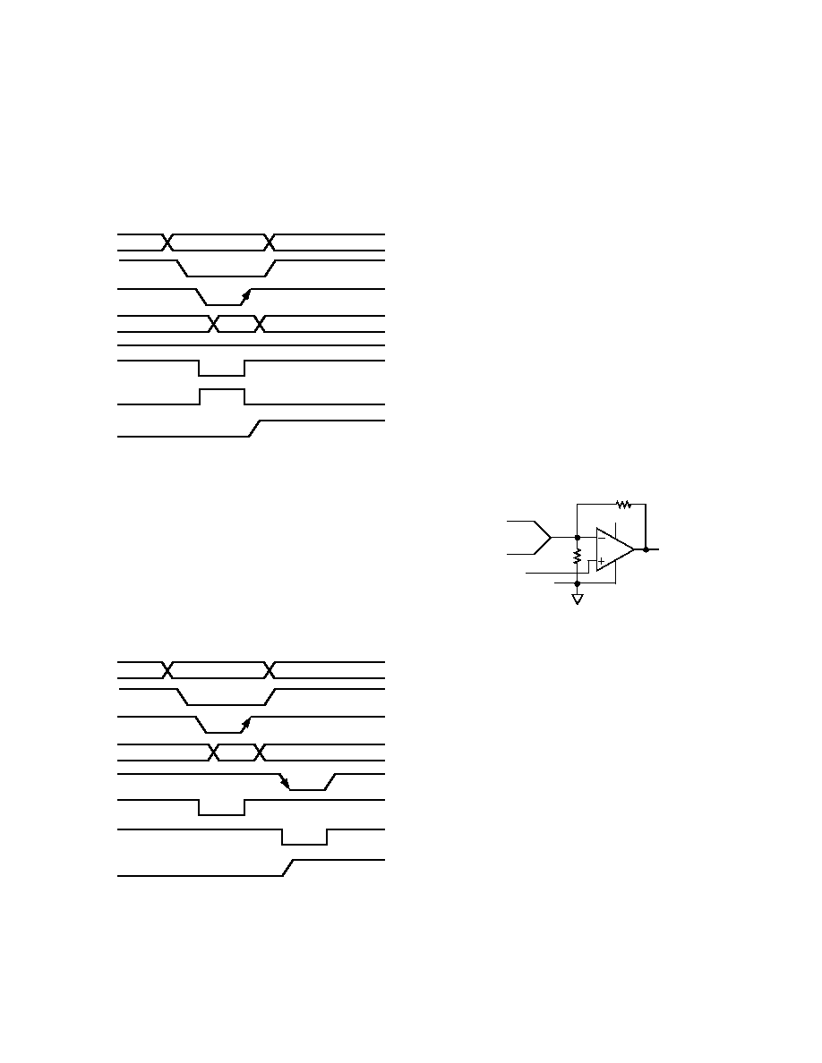
Automatic Update Mode
In this mode of operation the
LDAC signal is permanently tied
low. The state of the
LDAC is sampled on the rising edge of
WR. LDAC being low allows the selected DAC register to be
automatically updated on the rising edge of
WR. The output
update occurs on the rising edge of
WR. Figure 23 shows the
timing associated with the automatic update mode of operation
and also the status of the various registers during this frame.
A/B
CS
WR
D7–D0
LDAC = 0
HOLD
TRACK
I/P REG (MLE)
TRACK
HOLD
DAC REG (SLE)
TRACK
VOUT
Figure 23. Timing and Register Arrangement for Auto-
matic Update Mode
Simultaneous Update Mode
In this mode of operation the
LDAC signal is used to update both
DAC outputs simultaneously. The state of the
LDAC is sampled
on the rising edge of
WR. If LDAC is high, the automatic update
mode is disabled and both DAC latches are updated at any time
after the write by taking
LDAC low. The output update occurs
on the falling edge of
LDAC. LDAC must be taken back high
again before the next data transfer takes place. Figure 24
shows the timing associated with the simultaneous update mode
of operation and also the status of the various registers during
this frame.
A/B
CS
WR
D7–D0
LDAC
HOLD
TRACK
I/P REG (MLE)
TRACK
HOLD
DAC REG (SLE)
VOUT
HOLD
Figure 24. Timing and Register Arrangement for Simulta-
neous Update Mode
POWER-ON RESET
The AD7302 has a power-on reset circuit designed to allow
output stability during power-up. This circuit holds the DACs
in a reset state until a write takes place to the DAC. In the reset
state all zeros are latched into the input registers of each DAC
and the DAC registers are in transparent mode, thus the output
of both DACs is held at ground potential until a write takes
place to the DAC. The power-on reset circuitry generates a
PON STRB signal, which is a gating signal used within the logic
to identify a power-on condition.
POWER-DOWN FEATURES
The AD7302 has a power-down feature. This is implemented
by exercising the external
PD pin; an active low signal puts the
complete DAC into power-down mode. When in power-down
the current consumption of the device is reduced to 1
A max at
25
°C and 2 A max over temperature, making the device
suitable for use in portable battery powered equipment. When
power-down is activated, the reference bias servo loop and the
output amplifiers with their associated linear circuitry are
powered down, the reference resistors are open circuited to
further reduce the power consumption. The output sees a load
of approximately 23 k
to GND when in power-down mode as
shown in Figure 25. The contents of the data registers are
unaffected when in power-down mode. The device comes out
of power-down in typically 13
s (see Figure 10).
IDAC
11.7k
11.7k
VREF
VDD
Figure 25. Output Stage During Power-Down
Analog Outputs
The AD7302 contains two independent voltage output DACs
with 8-bit resolution and rail-to-rail operation. The output buffer
provides a gain of two at the output. Figures 2 to 4 show the
source and sink capabilities of the output amplifier. The slew
rate of the output amplifier is typically 7.5 V/
s and has a full-
scale settling to 8 bits with a 100 pF capacitive load in typically
1.2
s.
The input coding to the DAC is straight binary. Table I shows
the binary transfer function for the AD7302. Figure 26 shows
the DAC transfer function for binary coding. Any DAC output
voltage can be expressed as:
VOUT = 2
× V
REF (N/256)
where:
N
is the decimal equivalent of the binary input code.
N ranges from 0 to 255.
相关PDF资料 |
PDF描述 |
|---|---|
| AD7302BR-REEL7 | 2.7 V to 5.5 V, Parallel Input Dual Voltage Output 8-Bit DAC |
| AD7302BRUZ | 2.7 V to 5.5 V, Parallel Input Dual Voltage Output 8-Bit DAC |
| AD7302BRZ | 2.7 V to 5.5 V, Parallel Input Dual Voltage Output 8-Bit DAC |
| AD7303BNZ | +2.7 V to +5.5 V, Serial Input, Dual Voltage Output 8-Bit DAC |
| AD7306JR-REEL | LINE TRANSCEIVER, PDSO24 |
相关代理商/技术参数 |
参数描述 |
|---|---|
| AD7302BR | 功能描述:IC DAC 8BIT DUAL 2.7V 20-SOIC RoHS:否 类别:集成电路 (IC) >> 数据采集 - 数模转换器 系列:- 标准包装:2,400 系列:- 设置时间:- 位数:18 数据接口:串行 转换器数目:3 电压电源:模拟和数字 功率耗散(最大):- 工作温度:-40°C ~ 85°C 安装类型:表面贴装 封装/外壳:36-TFBGA 供应商设备封装:36-TFBGA 包装:带卷 (TR) 输出数目和类型:* 采样率(每秒):* |
| AD7302BR-REEL | 制造商:Analog Devices 功能描述:DAC 2-CH 8-bit 20-Pin SOIC W T/R 制造商:Rochester Electronics LLC 功能描述:3V/5V DUAL 8-BIT DAC I.C. - Tape and Reel |
| AD7302BR-REEL7 | 功能描述:IC DAC 8BIT DUAL R-R 20-SOIC RoHS:否 类别:集成电路 (IC) >> 数据采集 - 数模转换器 系列:- 产品培训模块:Lead (SnPb) Finish for COTS Obsolescence Mitigation Program 标准包装:50 系列:- 设置时间:4µs 位数:12 数据接口:串行 转换器数目:2 电压电源:单电源 功率耗散(最大):- 工作温度:-40°C ~ 85°C 安装类型:表面贴装 封装/外壳:8-TSSOP,8-MSOP(0.118",3.00mm 宽) 供应商设备封装:8-uMAX 包装:管件 输出数目和类型:2 电压,单极 采样率(每秒):* 产品目录页面:1398 (CN2011-ZH PDF) |
| AD7302BRU | 功能描述:IC DAC 8BIT DUAL R-R 20-TSSOP RoHS:否 类别:集成电路 (IC) >> 数据采集 - 数模转换器 系列:- 标准包装:2,400 系列:- 设置时间:- 位数:18 数据接口:串行 转换器数目:3 电压电源:模拟和数字 功率耗散(最大):- 工作温度:-40°C ~ 85°C 安装类型:表面贴装 封装/外壳:36-TFBGA 供应商设备封装:36-TFBGA 包装:带卷 (TR) 输出数目和类型:* 采样率(每秒):* |
| AD7302BRU-REEL | 制造商:Analog Devices 功能描述:DAC 2-CH 8-bit 20-Pin TSSOP T/R 制造商:Analog Devices 功能描述:DAC 2CH 8BIT 20TSSOP - Tape and Reel |
发布紧急采购,3分钟左右您将得到回复。