参数资料
| 型号: | AD7303BRZ |
| 厂商: | Analog Devices Inc |
| 文件页数: | 11/16页 |
| 文件大小: | 0K |
| 描述: | IC DAC 8BIT DUAL R-R 8-SOIC |
| 产品培训模块: | Data Converter Fundamentals DAC Architectures |
| 标准包装: | 98 |
| 设置时间: | 1.2µs |
| 位数: | 8 |
| 数据接口: | 串行 |
| 转换器数目: | 2 |
| 电压电源: | 单电源 |
| 功率耗散(最大): | 6.93mW |
| 工作温度: | -40°C ~ 105°C |
| 安装类型: | 表面贴装 |
| 封装/外壳: | 8-SOIC(0.154",3.90mm 宽) |
| 供应商设备封装: | 8-SOIC |
| 包装: | 管件 |
| 输出数目和类型: | 2 电压,单极;2 电压,双极 |
| 采样率(每秒): | 833k |
| 产品目录页面: | 784 (CN2011-ZH PDF) |
AD7303
–4–
REV. 0
ABSOLUTE MAXIMUM RATINGS*
(TA = +25°C unless otherwise noted)
VDD to GND . . . . . . . . . . . . . . . . . . . . . . . . . . –0.3 V to +7 V
Reference Input Voltage to GND . . . .
–0.3 V to VDD + 0.3 V
Digital Input Voltage to GND . . . . . . . –0.3 V to VDD + 0.3 V
VOUT A, VOUT B to GND . . . . . . . . . . . –0.3 V to VDD + 0.3 V
Operating Temperature Range
Commercial (B Version) . . . . . . . . . . . . . –40
°C to +105°C
Storage Temperature Range
. . . . . . . . . . . . –65
°C to +150°C
Junction Temperature . . . . . . . . . . . . . . . . . . . . . . . . . +150
°C
Plastic DIP Package, Power Dissipation . . . . . . . . . . 800 mW
θ
JA Thermal Impedance
. . . . . . . . . . . . . . . . . . . . . 117
°C/W
Lead Temperature (Soldering, 10 sec) . . . . . . . . . . . +260
°C
WARNING!
ESD SENSITIVE DEVICE
CAUTION
ESD (electrostatic discharge) sensitive device. Electrostatic charges as high as 4000 V readily
accumulate on the human body and test equipment and can discharge without detection.
Although the AD7303 features proprietary ESD protection circuitry, permanent damage may
occur on devices subjected to high energy electrostatic discharges. Therefore, proper ESD
precautions are recommended to avoid performance degradation or loss of functionality.
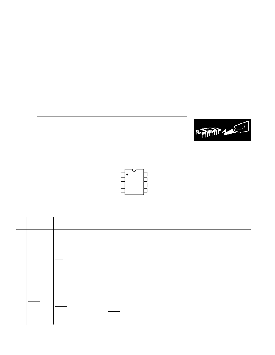
PIN CONFIGURATIONS
(DIP, SOIC and microSOIC)
1
2
3
4
8
7
6
5
TOP VIEW
(Not to Scale)
AD7303
VOUT A
SCLK
DIN
SYNC
VOUT B
VDD
GND
REF
PIN FUNCTION DESCRIPTIONS
Pin
No.
Mnemonic
Function
1VOUT A
Analog Output Voltage from DAC A. The output amplifier swings rail to rail on its output.
2VDD
Power Supply Input. These parts can be operated from +2.7 V to +5.5 V and should be decoupled to GND.
3
GND
Ground reference point for all circuitry on the part.
4
REF
External Reference Input. This can be used as the reference for both DACs, and is selected by setting the
INT
/EXT bit in the control register to a logic one. The range on this reference input is 1 V to VDD/2. When
the internal reference is selected, this voltage will appear as an output for decoupling purposes at the REF Pin.
When using the internal reference, external voltages should not be connected to the REF Pin, see Figure 21.
5
SCLK
Serial Clock. Logic Input. Data is clocked into the input shift register on the rising edge of the serial clock
input. Data can be transferred at rates up to 30 MHz.
6
DIN
Serial Data Input. This device has a 16-bit shift register, 8 bits for data and 8 bits for control. Data is clocked
into the register on the rising edge of the clock input.
7
SYNC
Level Triggered Control Input (active low). This is the frame synchronization signal for the input data. When
SYNC
goes low, it enables the input shift register and data is transferred in on the rising edges of the following
clocks. The rising edge of the SYNC causes the relevant registers to be updated.
8VOUT B
Analog output voltage from DAC B. The output amplifier swings rail to rail on its output.
SOIC Package, Power Dissipation . . . . . . . . . . . . . . . 450 mW
θ
JA Thermal Impedance
. . . . . . . . . . . . . . . . . . . . . 157
°C/W
Lead Temperature, Soldering
Vapor Phase (60 sec) . . . . . . . . . . . . . . . . . . . . . . +215
°C
Infrared (15 sec) . . . . . . . . . . . . . . . . . . . . . . . . . . +220
°C
MicroSOIC Package, Power Dissipation . . . . . . . . . . 450 mW
θ
JA Thermal Impedance
. . . . . . . . . . . . . . . . . . . . . 206
°C/W
Lead Temperature, Soldering
Vapor Phase (60 sec) . . . . . . . . . . . . . . . . . . . . . . +215
°C
Infrared (15 sec) . . . . . . . . . . . . . . . . . . . . . . . . . . +220
°C
*Stresses above those listed under “Absolute Maximum Ratings” may cause
permanent damage to the device. This is a stress rating only; functional operation
of the device at these or any other conditions above those listed in the operational
sections of this specification is not implied. Exposure to absolute maximum rating
conditions for extended periods may affect device reliability.
相关PDF资料 |
PDF描述 |
|---|---|
| VI-201-MY-F4 | CONVERTER MOD DC/DC 12V 50W |
| VE-BNX-MV-F3 | CONVERTER MOD DC/DC 5.2V 150W |
| VE-BNX-MV-F2 | CONVERTER MOD DC/DC 5.2V 150W |
| AD5441BRMZ | IC DAC 12BIT SERIAL IN 8MSOP |
| D38999/20SC4PC | CONN RCPT 4POS WALL MNT W/PINS |
相关代理商/技术参数 |
参数描述 |
|---|---|
| AD7303BRZ | 制造商:Analog Devices 功能描述:IC DAC 8BIT 833KSPS SOIC-8 |
| AD7303BRZ-REEL | 功能描述:IC DAC 8BIT DUAL R-R 8-SOIC RoHS:是 类别:集成电路 (IC) >> 数据采集 - 数模转换器 系列:- 产品培训模块:LTC263x 12-, 10-, and 8-Bit VOUT DAC Family 特色产品:LTC2636 - Octal 12-/10-/8-Bit SPI VOUT DACs with 10ppm/°C Reference 标准包装:91 系列:- 设置时间:4µs 位数:10 数据接口:MICROWIRE?,串行,SPI? 转换器数目:8 电压电源:单电源 功率耗散(最大):2.7mW 工作温度:-40°C ~ 85°C 安装类型:表面贴装 封装/外壳:14-WFDFN 裸露焊盘 供应商设备封装:14-DFN-EP(4x3) 包装:管件 输出数目和类型:8 电压,单极 采样率(每秒):* |
| AD7303BRZ-REEL7 | 功能描述:IC DAC 8BIT DUAL R-R 8-SOIC RoHS:是 类别:集成电路 (IC) >> 数据采集 - 数模转换器 系列:- 产品培训模块:LTC263x 12-, 10-, and 8-Bit VOUT DAC Family 特色产品:LTC2636 - Octal 12-/10-/8-Bit SPI VOUT DACs with 10ppm/°C Reference 标准包装:91 系列:- 设置时间:4µs 位数:10 数据接口:MICROWIRE?,串行,SPI? 转换器数目:8 电压电源:单电源 功率耗散(最大):2.7mW 工作温度:-40°C ~ 85°C 安装类型:表面贴装 封装/外壳:14-WFDFN 裸露焊盘 供应商设备封装:14-DFN-EP(4x3) 包装:管件 输出数目和类型:8 电压,单极 采样率(每秒):* |
| AD7304 | 制造商:AD 制造商全称:Analog Devices 功能描述:+3 V/+5 V, Rail-to-Rail Quad, 8-Bit DAC |
| AD7304BN | 制造商:Analog Devices 功能描述:IC 8BIT DAC 7304 DIP16 |
发布紧急采购,3分钟左右您将得到回复。