参数资料
| 型号: | AD7303BRZ |
| 厂商: | Analog Devices Inc |
| 文件页数: | 16/16页 |
| 文件大小: | 0K |
| 描述: | IC DAC 8BIT DUAL R-R 8-SOIC |
| 产品培训模块: | Data Converter Fundamentals DAC Architectures |
| 标准包装: | 98 |
| 设置时间: | 1.2µs |
| 位数: | 8 |
| 数据接口: | 串行 |
| 转换器数目: | 2 |
| 电压电源: | 单电源 |
| 功率耗散(最大): | 6.93mW |
| 工作温度: | -40°C ~ 105°C |
| 安装类型: | 表面贴装 |
| 封装/外壳: | 8-SOIC(0.154",3.90mm 宽) |
| 供应商设备封装: | 8-SOIC |
| 包装: | 管件 |
| 输出数目和类型: | 2 电压,单极;2 电压,双极 |
| 采样率(每秒): | 833k |
| 产品目录页面: | 784 (CN2011-ZH PDF) |
AD7303
–9–
REV. 0
grammed to transfer data in 16-bit words. After clocking all six-
teen bits to the shift register, the rising edge of SYNC executes
the programmed function. The DACs are double buffered
which allows their outputs to be simultaneously updated.
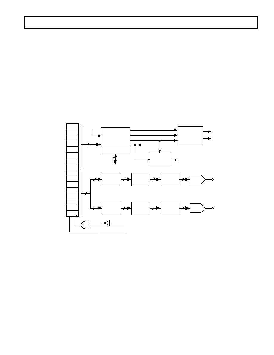
INPUT SHIFT REGISTER DESCRIPTION
The input shift register is 16 bits wide. The first eight bits con-
sist of control bits and the last eight bits are data bits. Figure 23
shows a block diagram of the logic interface on the AD7303
DAC. The seven bits in the control word are taken from the in-
put shift register to a latch sequencer that decodes this data and
provides output signals that control the data transfers to the in-
put and data registers of the selected DAC, as well as output
updating and various power-down features associated with the
control section. A description of all bits contained in the input
shift register is given below.
SERIAL INTERFACE
The AD7303 contains a versatile 3-wire serial interface that is
compatible with SPI, QSPI and Microwire interface stan-
dards as well as a host of digital signal processors. An active
low SYNC enables the shift register to receive data from the
serial data input DIN. Data is clocked into the shift register on
the rising edge of the serial clock. The serial clock frequency
can be as high as 30 MHz. This shift register is 16 bits wide as
shown in Figures 23 and 24. The first eight bits are control bits
and the second eight bits are data bits for the DACs. Each
transfer must consist of a 16-bit transfer. Data is sent MSB first
and can be transmitted in one 16-bit write or two 8-bit writes.
SPI and Microwire interfaces output data in 8-bit bytes and
thus require two 8-bit transfers. In this case the SYNC input to
the DAC should remain low until all sixteen bits have been
transferred to the shift register. QSPI interfaces can be pro-
DB0
DB1
DB2
DB3
DB4
DB5
DB6
DB7
INT/EXT
CR0
CR1
A/B
PDA
PDB
LDAC
X
8
LATCH
SEQUENCER
7
MSB
LSB
DAC A POWER-DOWN
DAC B POWER-DOWN
BANDGAP POWER-DOWN
LATCH & CLK
DRIVERS
16
REF
SELECTOR
INT
REFERENCE
CURRENT
SWITCH
CLOCK BUS
REF
RESISTOR
SWITCH
DAC A BIAS
DAC B BIAS
16-BIT
SHIFT
REGISTER
DIN
SYNC
DAC
REGISTER
30
DAC A
VOUT A
30
8 TO 32
DECODER
INPUT
REGISTER
8
SYNC
SCLK
BANDGAP
BIAS GEN
8
DAC
REGISTER
30
DAC B
VOUT B
30
8 TO 32
DECODER
INPUT
REGISTER
8
Figure 23. Logic Interface on the AD7303
相关PDF资料 |
PDF描述 |
|---|---|
| VI-201-MY-F4 | CONVERTER MOD DC/DC 12V 50W |
| VE-BNX-MV-F3 | CONVERTER MOD DC/DC 5.2V 150W |
| VE-BNX-MV-F2 | CONVERTER MOD DC/DC 5.2V 150W |
| AD5441BRMZ | IC DAC 12BIT SERIAL IN 8MSOP |
| D38999/20SC4PC | CONN RCPT 4POS WALL MNT W/PINS |
相关代理商/技术参数 |
参数描述 |
|---|---|
| AD7303BRZ | 制造商:Analog Devices 功能描述:IC DAC 8BIT 833KSPS SOIC-8 |
| AD7303BRZ-REEL | 功能描述:IC DAC 8BIT DUAL R-R 8-SOIC RoHS:是 类别:集成电路 (IC) >> 数据采集 - 数模转换器 系列:- 产品培训模块:LTC263x 12-, 10-, and 8-Bit VOUT DAC Family 特色产品:LTC2636 - Octal 12-/10-/8-Bit SPI VOUT DACs with 10ppm/°C Reference 标准包装:91 系列:- 设置时间:4µs 位数:10 数据接口:MICROWIRE?,串行,SPI? 转换器数目:8 电压电源:单电源 功率耗散(最大):2.7mW 工作温度:-40°C ~ 85°C 安装类型:表面贴装 封装/外壳:14-WFDFN 裸露焊盘 供应商设备封装:14-DFN-EP(4x3) 包装:管件 输出数目和类型:8 电压,单极 采样率(每秒):* |
| AD7303BRZ-REEL7 | 功能描述:IC DAC 8BIT DUAL R-R 8-SOIC RoHS:是 类别:集成电路 (IC) >> 数据采集 - 数模转换器 系列:- 产品培训模块:LTC263x 12-, 10-, and 8-Bit VOUT DAC Family 特色产品:LTC2636 - Octal 12-/10-/8-Bit SPI VOUT DACs with 10ppm/°C Reference 标准包装:91 系列:- 设置时间:4µs 位数:10 数据接口:MICROWIRE?,串行,SPI? 转换器数目:8 电压电源:单电源 功率耗散(最大):2.7mW 工作温度:-40°C ~ 85°C 安装类型:表面贴装 封装/外壳:14-WFDFN 裸露焊盘 供应商设备封装:14-DFN-EP(4x3) 包装:管件 输出数目和类型:8 电压,单极 采样率(每秒):* |
| AD7304 | 制造商:AD 制造商全称:Analog Devices 功能描述:+3 V/+5 V, Rail-to-Rail Quad, 8-Bit DAC |
| AD7304BN | 制造商:Analog Devices 功能描述:IC 8BIT DAC 7304 DIP16 |
发布紧急采购,3分钟左右您将得到回复。