- 您现在的位置:买卖IC网 > PDF目录1980 > AD7321BRUZ-REEL7 (Analog Devices Inc)IC ADC 12BIT+ SAR 2CHAN 14TSSOP PDF资料下载
参数资料
| 型号: | AD7321BRUZ-REEL7 |
| 厂商: | Analog Devices Inc |
| 文件页数: | 13/37页 |
| 文件大小: | 0K |
| 描述: | IC ADC 12BIT+ SAR 2CHAN 14TSSOP |
| 标准包装: | 1,000 |
| 位数: | 12 |
| 采样率(每秒): | 500k |
| 数据接口: | DSP,MICROWIRE?,QSPI?,串行,SPI? |
| 转换器数目: | 1 |
| 功率耗散(最大): | 17mW |
| 电压电源: | 双 ± |
| 工作温度: | -40°C ~ 85°C |
| 安装类型: | 表面贴装 |
| 封装/外壳: | 14-TSSOP(0.173",4.40mm 宽) |
| 供应商设备封装: | 14-TSSOP |
| 包装: | 带卷 (TR) |
| 输入数目和类型: | 2 个单端,单极;2 个单端,双极;1 个差分,单极;1 个差分,双极 |
| 配用: | EVAL-AD7321CBZ-ND - BOARD EVALUATION FOR AD7321 |
第1页第2页第3页第4页第5页第6页第7页第8页第9页第10页第11页第12页当前第13页第14页第15页第16页第17页第18页第19页第20页第21页第22页第23页第24页第25页第26页第27页第28页第29页第30页第31页第32页第33页第34页第35页第36页第37页
Data Sheet
AD7321
Rev. B | Page 19 of 36
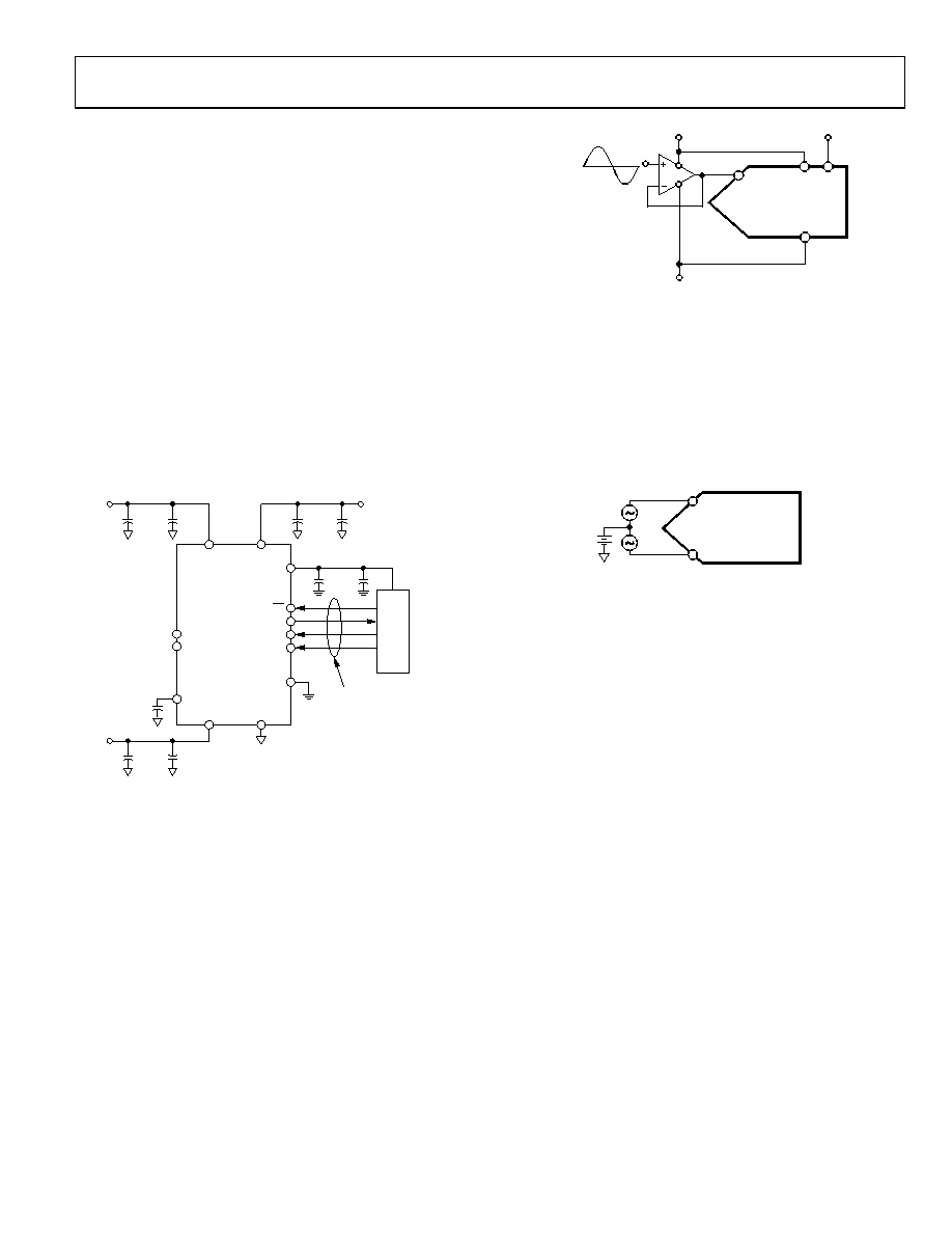
TYPICAL CONNECTION DIAGRAM
Figure 32 shows a typical connection diagram for the AD7321.
In this configuration, the AGND pin is connected to the analog
ground plane of the system, and the DGND pin is connected to
the digital ground plane of the system. The analog inputs on the
AD7321 are configured to operate in single-ended, true
differential, or pseudo differential mode. The AD7321 can operate
with either an internal or external reference. In Figure 32, the
AD7321 is configured to operate with the internal 2.5 V
reference. A 680 nF decoupling capacitor is required when
operating with the internal reference.
The VCC pin can be connected to either a 3 V supply voltage or a
5 V supply voltage. The VDD and VSS are the dual supplies for the
high voltage analog input structures. The voltage on these pins
must be equal to or greater than the highest analog input range
selected on the analog input channels (see Table 6). The VDRIVE
pin is connected to the supply voltage of the microprocessor.
The voltage applied to the VDRIVE input controls the voltage of
the serial interface. VDRIVE is set to 3 V or 5 V.
AD7321
VCC
VDD1
SERIAL
INTERFACE
C/P
VIN0
VIN1
REFIN/OUT
CS
DOUT
VDRIVE
SCLK
DIN
DGND
10F
0.1F
+
10F
0.1F
+
10F
0.1F
+
ANALOG INPUTS
±10V, ±5V, ±2.5V
0V TO +10V
+15V
–15V
680nF
VSS1
VCC + 2.7V TO 5.25V
1MINIMUM VDD AND VSS SUPPLY VOLTAGES
DEPEND ON THE HIGHEST ANALOG INPUT
RANGE SELECTED.
AGND
10F
0.1F
+
+3V SUPPLY
05399-
025
Figure 32. Typical Connection Diagram
ANALOG INPUT
Single-Ended Inputs
The AD7321 has a total of two analog inputs when operating
the AD7321 in single-ended mode. Each analog input is
independently programmed to one of the four analog input
ranges. In applications where the signal source is high
impedance, it is recommended to buffer the signal before
applying it to the ADC analog inputs. Figure 33 shows the
configuration of the AD7321 in single-ended mode.
AD73211
VIN+
V+
V–
VDD
VSS
VCC
5V
AGND
1ADDITIONAL PINS OMITTED FOR CLARITY.
05399-
026
Figure 33. Single-Ended Mode Typical Connection Diagram
True Differential Mode
The AD7321 can have one true differential analog input pair.
Differential signals have some benefits over single-ended
signals, including better noise immunity based on the common-
mode rejection of the device and improvements in distortion
performance. Figure 34 defines the configuration of the true
differential analog inputs of the AD7321.
AD73211
VIN+
VIN–
1ADDITIONAL PINS OMITTED FOR CLARITY.
05399-
027
Figure 34. True Differential Inputs
The amplitude of the differential signal is the difference
between the signals applied to the VIN+ and VIN pins in
each differential pair (VIN+ VIN). VIN+ and VIN should
be simultaneously driven by two signals each of amplitude
±4 × VREF (depending on the input range selected) that
are 180° out of phase. Assuming the ±4 × VREF mode, the
amplitude of the differential signal is 20 V to +20 V p-p
(2 × 4 × VREF), regardless of the common mode.
The common mode is the average of the two signals
(VIN+ + VIN)/2
and is, therefore, the voltage on which the two input signals are
centered.
This voltage is set up externally, and its range varies with
reference voltage. As the reference voltage increases, the
common-mode range decreases. When driving the differential
inputs with an amplifier, the actual common-mode range is
determined by the output swing of the amplifier. If the
differential inputs are not driven from an amplifier, the
common-mode range is determined by the supply voltage on
the VDD supply pin and the VSS supply pin.
When a conversion takes place, the common mode is rejected,
resulting in a noise-free signal of amplitude 2 × (4 × VREF) to
+2 × (4 × VREF) corresponding to digital codes 4096 to +4095.
相关PDF资料 |
PDF描述 |
|---|---|
| AD7322BRUZ-REEL7 | IC ADC 12BIT+ SAR 2CHAN 14TSSOP |
| AD7323BRUZ-REEL7 | IC ADC 12BIT+ SAR 4CHAN 16TSSOP |
| AD7324BRUZ-REEL | IC ADC 12BIT+SAR 4CHAN 16-TSSOP |
| AD7327BRUZ-REEL7 | IC ADC 12BIT+ SAR 8CHAN 20TSSOP |
| AD7328BRUZ-REEL | IC ADC 12BIT+SAR 8CHAN 20-TSSOP |
相关代理商/技术参数 |
参数描述 |
|---|---|
| AD7322 | 制造商:ATMEL 制造商全称:ATMEL Corporation 功能描述:Software Selectable True Bipolar Input, 2-Channel, 12-Bit Plus Sign ADC |
| AD7322BRU | 制造商:ATMEL 制造商全称:ATMEL Corporation 功能描述:Software Selectable True Bipolar Input, 2-Channel, 12-Bit Plus Sign ADC |
| AD7322BRUZ | 功能描述:IC ADC 12BIT+ SAR 2CHAN 14TSSOP RoHS:是 类别:集成电路 (IC) >> 数据采集 - 模数转换器 系列:- 标准包装:1 系列:microPOWER™ 位数:8 采样率(每秒):1M 数据接口:串行,SPI? 转换器数目:1 功率耗散(最大):- 电压电源:模拟和数字 工作温度:-40°C ~ 125°C 安装类型:表面贴装 封装/外壳:24-VFQFN 裸露焊盘 供应商设备封装:24-VQFN 裸露焊盘(4x4) 包装:Digi-Reel® 输入数目和类型:8 个单端,单极 产品目录页面:892 (CN2011-ZH PDF) 其它名称:296-25851-6 |
| AD7322BRUZ-REEL | 功能描述:IC ADC 12BIT+SAR 2CHAN 14-TSSOP RoHS:是 类别:集成电路 (IC) >> 数据采集 - 模数转换器 系列:- 标准包装:1,000 系列:- 位数:16 采样率(每秒):45k 数据接口:串行 转换器数目:2 功率耗散(最大):315mW 电压电源:模拟和数字 工作温度:0°C ~ 70°C 安装类型:表面贴装 封装/外壳:28-SOIC(0.295",7.50mm 宽) 供应商设备封装:28-SOIC W 包装:带卷 (TR) 输入数目和类型:2 个单端,单极 |
| AD7322BRUZ-REEL7 | 功能描述:IC ADC 12BIT+ SAR 2CHAN 14TSSOP RoHS:是 类别:集成电路 (IC) >> 数据采集 - 模数转换器 系列:- 标准包装:1,000 系列:- 位数:16 采样率(每秒):45k 数据接口:串行 转换器数目:2 功率耗散(最大):315mW 电压电源:模拟和数字 工作温度:0°C ~ 70°C 安装类型:表面贴装 封装/外壳:28-SOIC(0.295",7.50mm 宽) 供应商设备封装:28-SOIC W 包装:带卷 (TR) 输入数目和类型:2 个单端,单极 |
发布紧急采购,3分钟左右您将得到回复。