- 您现在的位置:买卖IC网 > PDF目录1980 > AD7321BRUZ-REEL7 (Analog Devices Inc)IC ADC 12BIT+ SAR 2CHAN 14TSSOP PDF资料下载
参数资料
| 型号: | AD7321BRUZ-REEL7 |
| 厂商: | Analog Devices Inc |
| 文件页数: | 9/37页 |
| 文件大小: | 0K |
| 描述: | IC ADC 12BIT+ SAR 2CHAN 14TSSOP |
| 标准包装: | 1,000 |
| 位数: | 12 |
| 采样率(每秒): | 500k |
| 数据接口: | DSP,MICROWIRE?,QSPI?,串行,SPI? |
| 转换器数目: | 1 |
| 功率耗散(最大): | 17mW |
| 电压电源: | 双 ± |
| 工作温度: | -40°C ~ 85°C |
| 安装类型: | 表面贴装 |
| 封装/外壳: | 14-TSSOP(0.173",4.40mm 宽) |
| 供应商设备封装: | 14-TSSOP |
| 包装: | 带卷 (TR) |
| 输入数目和类型: | 2 个单端,单极;2 个单端,双极;1 个差分,单极;1 个差分,双极 |
| 配用: | EVAL-AD7321CBZ-ND - BOARD EVALUATION FOR AD7321 |
第1页第2页第3页第4页第5页第6页第7页第8页当前第9页第10页第11页第12页第13页第14页第15页第16页第17页第18页第19页第20页第21页第22页第23页第24页第25页第26页第27页第28页第29页第30页第31页第32页第33页第34页第35页第36页第37页
AD7321
Data Sheet
Rev. B | Page 16 of 36
THEORY OF OPERATION
CIRCUIT INFORMATION
The AD7321 is a fast, 2-channel, 12-bit plus sign, bipolar input,
serial ADC. The AD7321 can accept bipolar input ranges that
include ±10 V, ±5 V, and ±2.5 V; it can also accept a 0 V to
+10 V unipolar input range. A different analog input range is
programmed on each analog input channel via the on-chip
registers. The AD7321 has a high speed serial interface that can
operate at throughput rates up to 500 kSPS.
voltage analog input structures. These supplies must be equal to
or greater than the largest analog input range selected. See Table 6
for the requirements of these supplies for each analog input range.
to power the ADC core.
Table 6. Reference and Supply Requirements for Each
Analog Input Range
Selected
Analog
Input
Range (V)
Reference
Voltage (V)
Full-Scale
Input
Range (V)
AVCC
(V)
Minimum
±10
2.5
±10
3/5
±10
3.0
±12
3/5
±12
±5
2.5
±5
3/5
±5
3.0
±6
3/5
±6
±2.5
2.5
±2.5
3/5
±5
3.0
±3
3/5
±5
0 to +10
2.5
0 to +10
3/5
+10/AGND
3.0
0 to +12
3/5
+12/AGND
1
Guaranteed performance for VDD = 12 V to 16.5 V and VSS = 12 V to 16.5 V.
The performance specifications are guaranteed for VDD = 12 V
to 16.5 V and VSS = 12 V to 16.5 V. With VDD and VSS supplies
outside this range, the AD7321 is fully functional but performance
is not guaranteed. When the AD7321 is configured with the
minimum VDD and VSS supplies, decrease the throughput rate to
meet the performance specifications (see the Typical Performance
Characteristics section). Figure 31 shows the change in THD as
the VDD and VSS supplies are reduced. For ac performance at the
maximum throughput rate, the THD degrades slightly as VDD and
VSS are reduced. It might therefore be necessary to reduce the
throughput rate when using minimum VDD and VSS supplies so
that there is less degradation of THD and the specified perfor-
mance is maintained. The degradation is due to an increase in
the on resistance of the input multiplexer when the VDD and VSS
supplies are reduced. Figure 18 and Figure 19 show the change
in INL and DNL as the VDD and VSS voltages are varied. For dc
performance when operating at the maximum throughput rate,
as the VDD and VSS supply voltages are reduced, the typical INL
and DNL error remains constant.
The analog inputs are configured as two single-ended inputs,
one true differential input pair or one pseudo differential input.
A selection is made by programming the mode bits, Mode 0
and Mode 1, in the control register.
The serial clock input accesses data from the part and provides
the clock source for the successive approximation ADC. The
AD7321 has an on-chip 2.5 V reference. However, the AD7321
can also work with an external reference. On power-up, the
external reference operation is the default option. If the internal
reference is the preferred option, the user must write to the
reference bit in the control register to select the internal
reference operation.
The AD7321 also features power-down options to allow power
savings between conversions. The power-down modes are
selected by programming the on-chip control register, as
described in the Modes of Operation section.
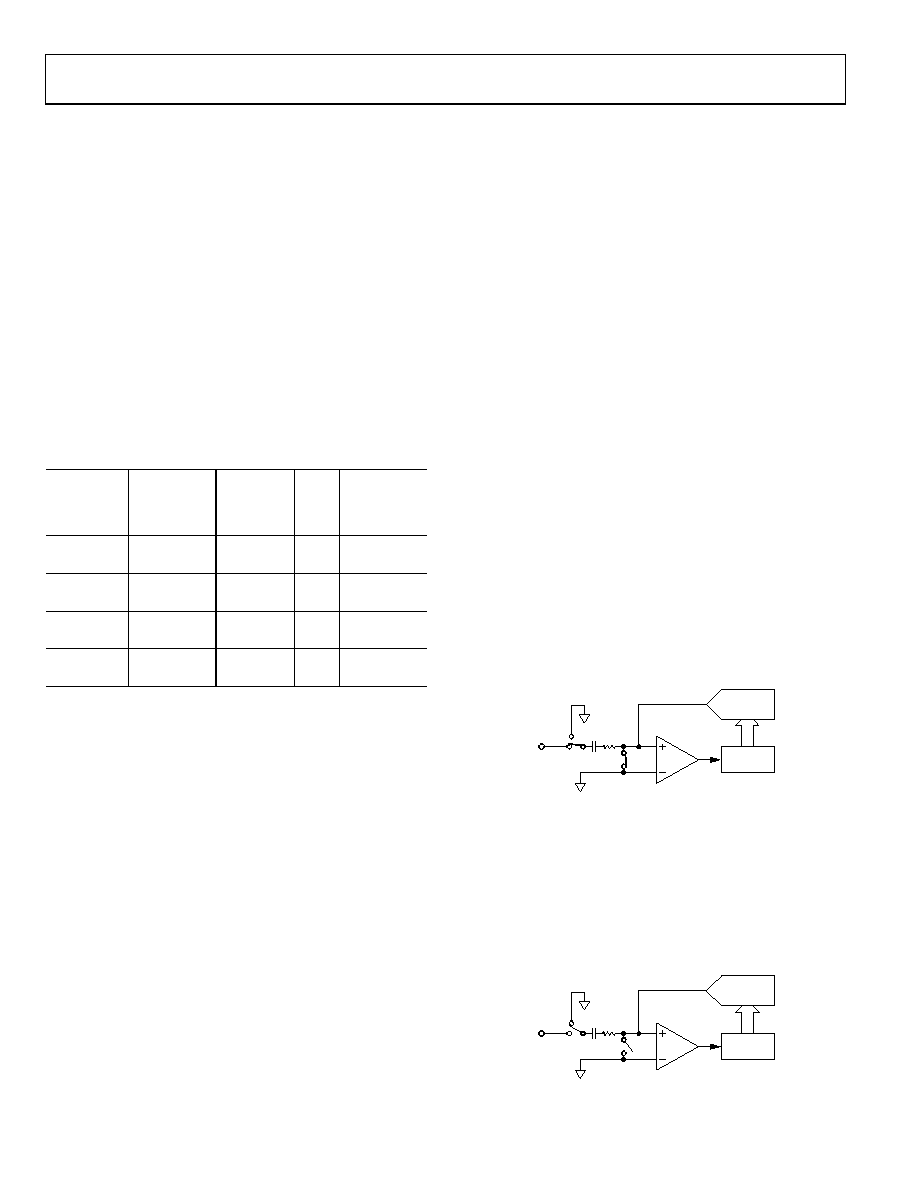
CONVERTER OPERATION
The AD7321 is a successive approximation analog-to-digital
converter built around two capacitive DACs. Figure 23 and
Figure 24 show simplified schematics of the ADC in single-
ended mode during the acquisition and conversion phases,
respectively. Figure 25 and Figure 26 show simplified
schematics of the ADC in differential mode during acquisition
and conversion phases, respectively. The ADC is composed of
control logic, a SAR, and capacitive DACs. In Figure 23 (the
acquisition phase), SW2 is closed and SW1 is in Position A, the
comparator is held in a balanced condition, and the sampling
capacitor array acquires the signal on the input.
CAPACITIVE
DAC
CONTROL
LOGIC
COMPARATOR
AGND
SW2
SW1
A
B
CS
VIN0
05399-
017
Figure 23. ADC Acquisition Phase (Single-Ended)
When the ADC starts a conversion (Figure 24), SW2 opens and
SW1 moves to Position B, causing the comparator to become
unbalanced. The control logic and the charge redistribution
DAC are used to add and subtract fixed amounts of charge from
the capacitive DAC to bring the comparator back into a
balanced condition. When the comparator is rebalanced, the
conversion is complete. The control logic generates the ADC
output code.
CAPACITIVE
DAC
CONTROL
LOGIC
COMPARATOR
AGND
SW2
SW1
A
B
CS
VIN0
05399-
018
Figure 24. ADC Conversion Phase (Single-Ended)
相关PDF资料 |
PDF描述 |
|---|---|
| AD7322BRUZ-REEL7 | IC ADC 12BIT+ SAR 2CHAN 14TSSOP |
| AD7323BRUZ-REEL7 | IC ADC 12BIT+ SAR 4CHAN 16TSSOP |
| AD7324BRUZ-REEL | IC ADC 12BIT+SAR 4CHAN 16-TSSOP |
| AD7327BRUZ-REEL7 | IC ADC 12BIT+ SAR 8CHAN 20TSSOP |
| AD7328BRUZ-REEL | IC ADC 12BIT+SAR 8CHAN 20-TSSOP |
相关代理商/技术参数 |
参数描述 |
|---|---|
| AD7322 | 制造商:ATMEL 制造商全称:ATMEL Corporation 功能描述:Software Selectable True Bipolar Input, 2-Channel, 12-Bit Plus Sign ADC |
| AD7322BRU | 制造商:ATMEL 制造商全称:ATMEL Corporation 功能描述:Software Selectable True Bipolar Input, 2-Channel, 12-Bit Plus Sign ADC |
| AD7322BRUZ | 功能描述:IC ADC 12BIT+ SAR 2CHAN 14TSSOP RoHS:是 类别:集成电路 (IC) >> 数据采集 - 模数转换器 系列:- 标准包装:1 系列:microPOWER™ 位数:8 采样率(每秒):1M 数据接口:串行,SPI? 转换器数目:1 功率耗散(最大):- 电压电源:模拟和数字 工作温度:-40°C ~ 125°C 安装类型:表面贴装 封装/外壳:24-VFQFN 裸露焊盘 供应商设备封装:24-VQFN 裸露焊盘(4x4) 包装:Digi-Reel® 输入数目和类型:8 个单端,单极 产品目录页面:892 (CN2011-ZH PDF) 其它名称:296-25851-6 |
| AD7322BRUZ-REEL | 功能描述:IC ADC 12BIT+SAR 2CHAN 14-TSSOP RoHS:是 类别:集成电路 (IC) >> 数据采集 - 模数转换器 系列:- 标准包装:1,000 系列:- 位数:16 采样率(每秒):45k 数据接口:串行 转换器数目:2 功率耗散(最大):315mW 电压电源:模拟和数字 工作温度:0°C ~ 70°C 安装类型:表面贴装 封装/外壳:28-SOIC(0.295",7.50mm 宽) 供应商设备封装:28-SOIC W 包装:带卷 (TR) 输入数目和类型:2 个单端,单极 |
| AD7322BRUZ-REEL7 | 功能描述:IC ADC 12BIT+ SAR 2CHAN 14TSSOP RoHS:是 类别:集成电路 (IC) >> 数据采集 - 模数转换器 系列:- 标准包装:1,000 系列:- 位数:16 采样率(每秒):45k 数据接口:串行 转换器数目:2 功率耗散(最大):315mW 电压电源:模拟和数字 工作温度:0°C ~ 70°C 安装类型:表面贴装 封装/外壳:28-SOIC(0.295",7.50mm 宽) 供应商设备封装:28-SOIC W 包装:带卷 (TR) 输入数目和类型:2 个单端,单极 |
发布紧急采购,3分钟左右您将得到回复。