- 您现在的位置:买卖IC网 > PDF目录10302 > AD7322BRUZ-REEL (Analog Devices Inc)IC ADC 12BIT+SAR 2CHAN 14-TSSOP PDF资料下载
参数资料
| 型号: | AD7322BRUZ-REEL |
| 厂商: | Analog Devices Inc |
| 文件页数: | 13/37页 |
| 文件大小: | 0K |
| 描述: | IC ADC 12BIT+SAR 2CHAN 14-TSSOP |
| 标准包装: | 2,500 |
| 位数: | 12 |
| 采样率(每秒): | 1M |
| 数据接口: | DSP,MICROWIRE?,QSPI?,串行,SPI? |
| 转换器数目: | 1 |
| 功率耗散(最大): | 30mW |
| 电压电源: | 双 ± |
| 工作温度: | -40°C ~ 85°C |
| 安装类型: | 表面贴装 |
| 封装/外壳: | 14-TSSOP(0.173",4.40mm 宽) |
| 供应商设备封装: | 14-TSSOP |
| 包装: | 带卷 (TR) |
| 输入数目和类型: | 2 个单端,单极;2 个单端,双极;1 个差分,单极;1 个差分,双极 |
| 配用: | EVAL-AD7322CBZ-ND - BOARD EVALUATION FOR AD7322 |
第1页第2页第3页第4页第5页第6页第7页第8页第9页第10页第11页第12页当前第13页第14页第15页第16页第17页第18页第19页第20页第21页第22页第23页第24页第25页第26页第27页第28页第29页第30页第31页第32页第33页第34页第35页第36页第37页
Data Sheet
AD7322
Rev. B | Page 19 of 36
When a conversion takes place, the common mode is rejected,
resulting in a noise-free signal of amplitude 2 × (4 × VREF) to
+2 × (4 × VREF), corresponding to Digital Code 4096 to
Digital Code +4095.
±16.5V VDD/VSS
±12V VDD/VSS
5
–6
V
CO
M
RANG
E
(
V
)
4
3
2
1
0
–1
–2
–3
–4
–5
VCC = 3V
VREF = 3V
±2.5V
RANGE
±10V
RANGE
±5V RANGE
±2.5V
RANGE
±5V RANGE
±10V
RANGE
04863-
045
Figure 35. Common-Mode Range for VCC = 3 V and REFIN/OUT = 3 V
±16.5V VDD/VSS
±12V VDD/VSS
V
CO
M
RANG
E
(
V
)
VCC = 5V
VREF = 3V
8
–4
6
4
2
0
–2
±2.5V
RANGE
±10V
RANGE
±5V RANGE
±2.5V
RANGE
±5V RANGE
±10V
RANGE
04863-
046
Figure 36. Common-Mode Range for VCC = 5 V and REFIN/OUT = 3 V
6
–8
4
2
0
–2
–4
–6
±16.5V VDD/VSS
±12V VDD/VSS
V
CO
M
RANG
E
(
V
)
VCC = 3V
VREF = 2.5V
±2.5V
RANGE
±10V
RANGE
±5V RANGE
±2.5V
RANGE
±5V RANGE
±10V
RANGE
04863-
047
Figure 37. Common-Mode Range for VCC = 3 V and REFIN/OUT = 2.5 V
8
–8
6
4
2
0
–2
–4
–6
±16.5V VDD/VSS
±12V VDD/VSS
V
CO
M
RANG
E
(
V
)
VCC = 5V
VREF = 2.5V
±2.5V
RANGE
±10V
RANGE
±5V RANGE
±2.5V
RANGE
±5V RANGE
±10V
RANGE
04863-
048
Figure 38. Common-Mode Range for VCC = 5 V and REFIN/OUT = 2.5 V
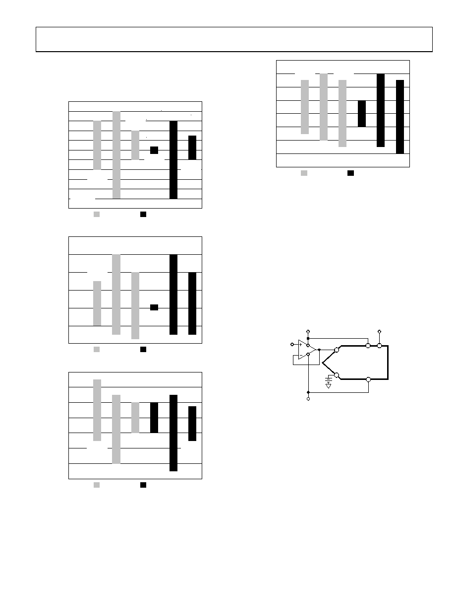
Pseudo Differential Inputs
input is coupled to the signal source and must have an amplitude
within the selected range for that channel as programmed in the
range register. A dc input is applied to the VIN input. The voltage
applied to this input provides an offset for the VIN+ input from
ground or a pseudo ground. Pseudo differential inputs separate
the analog input signal ground from the ADC ground, allowing
cancellation of dc common-mode voltages. Figure 39 shows the
AD7322 configured in pseudo differential mode.
When a conversion takes place, the pseudo ground corresponds
to Code 4096 and the maximum amplitude corresponds to
Code +4095.
AD73221
VIN+
V+
V–
VDD
VSS
VCC
5V
VIN–
04863-
028
1ADDITIONAL PINS OMITTED FOR CLARITY.
NOTES
1. VIN+ REFERS TO VIN0 AND VIN– REFERS TO VIN1.
Figure 39. Pseudo Differential Inputs
Figure 40 and Figure 41 show the typical voltage range on the
VIN input for the different analog input ranges when
configured in the pseudo differential mode.
For example, when the AD7322 is configured to operate in
pseudo differential mode and the ±5 V range is selected with
±16.5 V VDD/VSS supplies and 5 V VCC, the voltage on the VIN
input can vary from 6.5 V to +6.5 V.
相关PDF资料 |
PDF描述 |
|---|---|
| VE-BTV-MW-S | CONVERTER MOD DC/DC 5.8V 100W |
| VE-23K-MY | CONVERTER MOD DC/DC 40V 50W |
| VE-24W-CU-S | CONVERTER MOD DC/DC 5.5V 200W |
| VE-23J-MY | CONVERTER MOD DC/DC 36V 50W |
| VE-B4H-MW-S | CONVERTER MOD DC/DC 52V 100W |
相关代理商/技术参数 |
参数描述 |
|---|---|
| AD7322BRUZ-REEL7 | 功能描述:IC ADC 12BIT+ SAR 2CHAN 14TSSOP RoHS:是 类别:集成电路 (IC) >> 数据采集 - 模数转换器 系列:- 标准包装:1,000 系列:- 位数:16 采样率(每秒):45k 数据接口:串行 转换器数目:2 功率耗散(最大):315mW 电压电源:模拟和数字 工作温度:0°C ~ 70°C 安装类型:表面贴装 封装/外壳:28-SOIC(0.295",7.50mm 宽) 供应商设备封装:28-SOIC W 包装:带卷 (TR) 输入数目和类型:2 个单端,单极 |
| AD7322LYRU | 制造商:Analog Devices 功能描述: |
| AD7323 | 制造商:AD 制造商全称:Analog Devices 功能描述:500 kSPS, 4-Channel, Software-Selectable, True Bipolar Input, 12-Bit Plus Sign ADC |
| AD7323BRUZ | 功能描述:IC ADC 12BIT+ SAR 4CHAN 16TSSOP RoHS:是 类别:集成电路 (IC) >> 数据采集 - 模数转换器 系列:- 标准包装:1 系列:microPOWER™ 位数:8 采样率(每秒):1M 数据接口:串行,SPI? 转换器数目:1 功率耗散(最大):- 电压电源:模拟和数字 工作温度:-40°C ~ 125°C 安装类型:表面贴装 封装/外壳:24-VFQFN 裸露焊盘 供应商设备封装:24-VQFN 裸露焊盘(4x4) 包装:Digi-Reel® 输入数目和类型:8 个单端,单极 产品目录页面:892 (CN2011-ZH PDF) 其它名称:296-25851-6 |
| AD7323BRUZ-REEL | 功能描述:IC ADC 12BIT+SAR 4CHAN 16-TSSOP RoHS:是 类别:集成电路 (IC) >> 数据采集 - 模数转换器 系列:- 标准包装:1,000 系列:- 位数:16 采样率(每秒):45k 数据接口:串行 转换器数目:2 功率耗散(最大):315mW 电压电源:模拟和数字 工作温度:0°C ~ 70°C 安装类型:表面贴装 封装/外壳:28-SOIC(0.295",7.50mm 宽) 供应商设备封装:28-SOIC W 包装:带卷 (TR) 输入数目和类型:2 个单端,单极 |
发布紧急采购,3分钟左右您将得到回复。