- 您现在的位置:买卖IC网 > PDF目录10296 > AD7366BRUZ-5-RL7 (Analog Devices Inc)IC ADC 12BIT DUAL BIPO 24-TSSOP PDF资料下载
参数资料
| 型号: | AD7366BRUZ-5-RL7 |
| 厂商: | Analog Devices Inc |
| 文件页数: | 9/28页 |
| 文件大小: | 0K |
| 描述: | IC ADC 12BIT DUAL BIPO 24-TSSOP |
| 设计资源: | Driving the AD7366/7 Bipolar SAR ADC in Low-Distortion DC-Coupled Appls (CN0042) |
| 标准包装: | 1,000 |
| 系列: | iCMOS® |
| 位数: | 12 |
| 采样率(每秒): | 500k |
| 数据接口: | DSP,MICROWIRE?,QSPI?,串行,SPI? |
| 转换器数目: | 2 |
| 功率耗散(最大): | 88.8mW |
| 电压电源: | 模拟和数字,双 ± |
| 工作温度: | -40°C ~ 85°C |
| 安装类型: | 表面贴装 |
| 封装/外壳: | 24-TSSOP(0.173",4.40mm 宽) |
| 供应商设备封装: | 24-TSSOP |
| 包装: | 带卷 (TR) |
| 输入数目和类型: | 4 个单端,单极;4 个单端,双极 |
| 配用: | EVAL-AD7366CBZ-ND - BOARD EVALUATION FOR AD7366 |
第1页第2页第3页第4页第5页第6页第7页第8页当前第9页第10页第11页第12页第13页第14页第15页第16页第17页第18页第19页第20页第21页第22页第23页第24页第25页第26页第27页第28页
AD7366-5/AD7367-5
Rev. A | Page 17 of 28
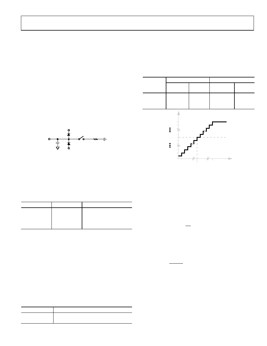
ANALOG INPUTS
Each ADC in the AD7366-5/AD7367-5 has two single-ended
analog inputs. Figure 18 shows the equivalent circuit of the
analog input structure of the AD7366-5/AD7367-5. The two
diodes provide ESD protection. Care must be taken to ensure
that the analog input signals never exceed the supply rails by
more than 300 mV. Otherwise, these diodes become forward-
biased and start conducting current into the substrate. The
diodes can conduct up to 10 mA without causing irreversible
damage to the part. The resistors are lumped components made
up of the on resistance of the switches. The value of these resistors
is typically 170 Ω. Capacitor C1 can primarily be attributed to
pin capacitance while Capacitor C2 is the sampling capacitor of
the ADC. The total lumped capacitance of C1 and C2 is approxi-
mately 9 pF for the ±10 V input range and approximately 13 pF
for all other input ranges.
D
VDD
C2
R1
VIN0
VSS
C1
0
68
42
-02
0
Figure 18. Equivalent Analog Input Structure
The AD7366-5/AD7367-5 can handle true bipolar input voltages.
The analog input can be set to one of three ranges: ±10 V, ±5 V, or
0 V to +10 V. The logic levels on Pin RANGE0 and Pin RANGE1
determine which input range is selected as outlined in Table 8.
These range bits should not be changed during the acquisition
time prior to a conversion, but can change at any other time.
Table 8. Analog Input Range Selection
RANGE0
RANGE1
Range Selected
0
±10 V
1
0
±5 V
0
1
0 V to +10 V
1
Do not program
The parts require VDD and VSS dual supplies for the high voltage
analog input structures. These supplies must be greater than or
equal to ±5 V (see Table 7 for the requirements on these supplies).
The AD7366-5/AD7367-5 require a low voltage 4.75 V to 5.25 V
AVCC supply to power the ADC core, a 4.75 V to 5.25 V DVCC
supply for digital power, and a 2.7 V to 5.25 V VDRIVE supply for
interface power.
Channel selection is made via the ADDR pin as shown in Table 9.
The logic level on the ADDR pin is latched on the rising edge of
the BUSY signal for the next conversion, not the one in progress.
When power is first supplied to the AD7366-5/AD7367-5, the
default channel selection is VA1 and VB1.
Table 9. Channel Selection
ADDR
Channels Selected
0
VA1, VB1
1
VA2, VB2
TRANSFER FUNCTION
The output coding of the AD7366-5/AD7367-5 is twos comple-
ment. The designed code transitions occur at successive integer
LSB values (that is, 1 LSB, 2 LSB, and so on). The LSB size is
dependent on the analog input range selected (see Table 10).
The ideal transfer characteristic is shown in Figure 19.
Table 10. LSB Sizes for Each Analog Input Range
Input
Range
AD7366-5
AD7367-5
Full-Scale
Range
LSB Size
(mV)
Full-Scale
Range
LSB Size
(mV)
±10 V
20 V/4096
4.88
20 V/16384
1.22
±5 V
10 V/4096
2.44
10 V/16384
0.61
0 V to +10 V
10 V/4096
2.44
10 V/16384
0.61
+FSR/2 – 1LSB
ANALOG INPUT
0V
ADC
CO
DE
011...111
011...110
000...001
000...000
111...111
100...010
100...001
100...000
–FSR/2 + 1LSB
06
84
2-
0
21
Figure 19. Transfer Characteristic
Track-and-Hold
The track-and-hold on the analog input of the AD7366-5/
AD7367-5 allows the ADC to accurately convert an input sine
wave of full-scale amplitude to 12-/14-bit accuracy. The input
bandwidth of the track-and-hold is greater than the Nyquist
rate of the ADC. The AD7366-5/AD7367-5 can handle
frequencies up to 35 MHz.
The track-and-hold enters its tracking mode once the BUSY
signal goes low after the CS falling edge. The time required to
acquire an input signal depends on how quickly the sampling
capacitor is charged. With zero source impedance, 140 ns is
sufficient to acquire the signal to the 12-bit level for the AD7366-5
and the 14-bit level for the AD7367-5. The acquisition time for
the ±10 V, ±5 V, and 0 V to +10 V ranges to settle to within ± LSB
is typically 140 ns. The ADC goes back into hold mode on the
falling edge of CNVST.
The acquisition time required is calculated using the following
formula:
tACQ = 10 × ((RSOURCE + R) × C)
where:
C is the sampling capacitance.
R is the resistance seen by the track-and-hold amplifier looking
at the input.
RSOURCE should include any extra source impedance on the
analog input.
相关PDF资料 |
PDF描述 |
|---|---|
| MS27467E21B11BA | CONN HSG PLUG 11POS STRGHT SCKT |
| D38999/26MD19SNLC | CONN HSG PLUG 19POS STRGHT SCKT |
| MS27497E12F4P | CONN RCPT 4POS WALL MNT W/PINS |
| D38999/20FJ37SNLC | CONN HSG RCPT 37POS WALL MT SCKT |
| AD7799BRU-REEL | IC ADC 24BIT 3CH LP 16-TSSOP |
相关代理商/技术参数 |
参数描述 |
|---|---|
| AD7366BRUZ-REEL7 | 制造商:AD 制造商全称:Analog Devices 功能描述:True Bipolar Input, Dual 1us, 12-Bit, 2-Channel SAR ADC |
| AD7366BRUZ-RL7 | 功能描述:IC ADC 12BIT SAR 1MSPS 24TSSOP RoHS:是 类别:集成电路 (IC) >> 数据采集 - 模数转换器 系列:iCMOS® 标准包装:1,000 系列:- 位数:16 采样率(每秒):45k 数据接口:串行 转换器数目:2 功率耗散(最大):315mW 电压电源:模拟和数字 工作温度:0°C ~ 70°C 安装类型:表面贴装 封装/外壳:28-SOIC(0.295",7.50mm 宽) 供应商设备封装:28-SOIC W 包装:带卷 (TR) 输入数目和类型:2 个单端,单极 |
| AD7367 | 制造商:AD 制造商全称:Analog Devices 功能描述:True Bipolar Input, Dual 1 レs, 12-/14-Bit, 2-Channel SAR ADCs |
| AD7367-5 | 制造商:AD 制造商全称:Analog Devices 功能描述:True Bipolar Input, Dual 1 レs, 12-/14-Bit, 2-Channel SAR ADCs |
| AD7367-5ARUZ | 制造商:AD 制造商全称:Analog Devices 功能描述:1 MSPS, 8-Channel, Software-Selectable, True Bipolar Input, 12-Bit Plus Sign ADC |
发布紧急采购,3分钟左右您将得到回复。