- 您现在的位置:买卖IC网 > PDF目录10674 > AD7366BRUZ (Analog Devices Inc)IC ADC 12BIT SAR 1MSPS 24TSSOP PDF资料下载
参数资料
| 型号: | AD7366BRUZ |
| 厂商: | Analog Devices Inc |
| 文件页数: | 13/29页 |
| 文件大小: | 0K |
| 描述: | IC ADC 12BIT SAR 1MSPS 24TSSOP |
| 设计资源: | Driving the AD7366/7 Bipolar SAR ADC in Low-Distortion DC-Coupled Appls (CN0042) |
| 标准包装: | 62 |
| 系列: | iCMOS® |
| 位数: | 12 |
| 采样率(每秒): | 1M |
| 数据接口: | DSP,MICROWIRE?,QSPI?,串行,SPI? |
| 转换器数目: | 2 |
| 功率耗散(最大): | 88.8mW |
| 电压电源: | 模拟和数字,双 ± |
| 工作温度: | -40°C ~ 85°C |
| 安装类型: | 表面贴装 |
| 封装/外壳: | 24-TSSOP(0.173",4.40mm 宽) |
| 供应商设备封装: | 24-TSSOP |
| 包装: | 管件 |
| 输入数目和类型: | 4 个单端,单极;4 个单端,双极 |
| 产品目录页面: | 777 (CN2011-ZH PDF) |
| 配用: | EVAL-AD7366CBZ-ND - BOARD EVALUATION FOR AD7366 |
第1页第2页第3页第4页第5页第6页第7页第8页第9页第10页第11页第12页当前第13页第14页第15页第16页第17页第18页第19页第20页第21页第22页第23页第24页第25页第26页第27页第28页第29页
AD7366/AD7367
Rev. D | Page 19 of 28
DRIVER AMPLIFIER CHOICE
The AD7366/AD7367 have a total of four analog inputs, which
operate in single-ended mode. The analog inputs for both ADCs
can be programmed to one of the three analog input ranges. In
applications where the signal source is high impedance, it is
recommended that the signal be buffered before applying it to
the ADC analog inputs. Figure 21 shows the configuration of
the AD7366/AD7367 in single-ended mode.
In applications where the THD and SNR are critical specifi-
cations, the analog input of the AD7366/AD7367 should be
driven from a low impedance source. Large source impedances
significantly affect the ac performance of the ADC and can
necessitate the use of an input buffer amplifier.
When no amplifier is used to drive the analog input, the source
impedance should be limited to low values. The maximum source
impedance depends on the amount of THD that can be tolerated
in the application. The THD increases as the source impedance
increases and performance degrades. Figure 7 shows THD vs.
the analog input frequency for various source impedances.
Depending on the input range and analog input configuration
selected, the AD7366/AD7367 can handle source impedances as
illustrated in Figure 7.
Due to the programmable nature of the analog inputs on the
AD7366/AD7367, the choice of op amp used to drive the
inputs is a function of the particular application and depends
on the analog input voltage range selected.
The driver amplifier must be able to settle for a full-scale step
to a 14-bit level, 0.0061%, in less than the specified acquisition
time of the AD7366/AD7367. An op amp such as the AD8021
meets this requirement when operating in single-ended mode.
The AD8021 needs an external compensating NPO type of
capacitor. The AD8022 can also be used in high frequency
applications where a dual version is required. For lower fre-
quency applications, recommended op amps are the AD797,
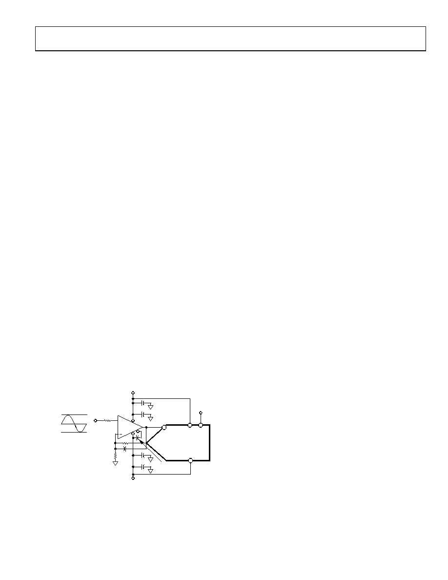
V+
V–
VDD
VSS
VA1
VCC
+5V
AGND
AD8021
1k
1k
15pF
CCOMP = 10pF
–10V/–5V
+10V/+5V
AD7366/
AD7367*
*ADDITIONAL PINS OMITTED FOR CLARITY.
10F
+
0.1F
+
0.1F
+
10F
+
06703-
023
Figure 21. Typical Connection Diagram with the AD8021 for Driving the
Analog Input
VDRIVE
The AD7366/AD7367 also have a VDRIVE feature to control the
voltage at which the serial interface operates. VDRIVE allows the
ADC to easily interface to both 3 V and 5 V processors. For
example, if the AD7366/AD7367 were operated with a VCC of
5 V, the VDRIVE pin could be powered from a 3 V supply, allowing
a large dynamic range with low voltage digital processors. Thus,
the AD7366/AD7367 can be used with the ±10 V input range
while still being able to interface to 3 V digital parts.
To achieve the maximum throughput rate of 1.12 MSPS for the
AD7366 or 1 MSPS for the AD7367, VDRIVE must be greater than
or equal to 4.75 V (see Table 2 and Table 3). The maximum
throughput rate with the VDRIVEvoltage set to less than 4.75 V
and greater than 2.7 V is 1 MSPS for the AD7366 and 900 kSPS
for the AD7367.
REFERENCE
The AD7366/AD7367 can operate with either the internal 2.5 V
on-chip reference or an externally applied reference. The logic
state of the REFSEL pin determines whether the internal refer-
ence is used. The internal reference is selected for both ADCs
when the REFSEL pin is tied to logic high. If the REFSEL pin is
tied to GND, an external reference can be supplied through the
DCAPA and DCAPB pins. On power-up, the REFSEL pin must be
tied to either a low or high logic state for the part to operate.
Suitable reference sources for the AD7366/AD7367 include the
The internal reference circuitry consists of a 2.5 V band gap
reference and a reference buffer. When operating the AD7366/
AD7367 in internal reference mode, the 2.5 V internal reference
is available at the DCAPA and DCAPB pins, which should be
decoupled to AGND using a 680 nF capacitor. It is recom-
mended that the internal reference be buffered before applying
it elsewhere in the system. The internal reference is capable of
sourcing up to 150 μA with an analog input range of ±10 V
and 70 μA for both the ±5 V and 0 V to 10 V ranges.
If the internal reference operation is required for the ADC con-
version, the REFSEL pin must be tied to logic high on power-up.
The reference buffer requires 70 s to power up and charge the
680 nF decoupling capacitor during the power-up time.
The AD7366/AD7367 are specified for a 2.5 V to 3 V reference.
When a 3 V reference is selected, the analog input ranges are
±12 V, ±6 V, and 0 V to 12 V. For these ranges, the VDD supply
must be greater than or equal to +12 V and the VSS supply must
be less than or equal to 12 V.
相关PDF资料 |
PDF描述 |
|---|---|
| AD7866ARUZ | IC ADC 12BIT 2CH DUAL 20-TSSOP |
| AD7190BRUZ | IC ADC 2CH 24BIT W/PGA 24TSSOP |
| AD7715ARZ-5 | IC ADC 16BIT SIGMA-DELTA 16-SOIC |
| AD7766BRUZ-2 | IC ADC 24BIT 32KSPS SAR 16TSSOP |
| LM2901VDG | IC COMP QUAD SGL SUPPLY 14SOIC |
相关代理商/技术参数 |
参数描述 |
|---|---|
| AD7366BRUZ-5 | 功能描述:IC ADC 12BIT DUAL 500KSPS 24-TSS RoHS:是 类别:集成电路 (IC) >> 数据采集 - 模数转换器 系列:iCMOS® 其它有关文件:TSA1204 View All Specifications 标准包装:1 系列:- 位数:12 采样率(每秒):20M 数据接口:并联 转换器数目:2 功率耗散(最大):155mW 电压电源:模拟和数字 工作温度:-40°C ~ 85°C 安装类型:表面贴装 封装/外壳:48-TQFP 供应商设备封装:48-TQFP(7x7) 包装:Digi-Reel® 输入数目和类型:4 个单端,单极;2 个差分,单极 产品目录页面:1156 (CN2011-ZH PDF) 其它名称:497-5435-6 |
| AD7366BRUZ-500RL7 | 功能描述:IC ADC 12BIT SAR 1MSPS 24TSSOP RoHS:是 类别:集成电路 (IC) >> 数据采集 - 模数转换器 系列:iCMOS® 标准包装:1,000 系列:- 位数:16 采样率(每秒):45k 数据接口:串行 转换器数目:2 功率耗散(最大):315mW 电压电源:模拟和数字 工作温度:0°C ~ 70°C 安装类型:表面贴装 封装/外壳:28-SOIC(0.295",7.50mm 宽) 供应商设备封装:28-SOIC W 包装:带卷 (TR) 输入数目和类型:2 个单端,单极 |
| AD7366BRUZ-5500RL7 | 功能描述:IC ADC 12BIT DUAL BIPO 24-TSSOP RoHS:是 类别:集成电路 (IC) >> 数据采集 - 模数转换器 系列:iCMOS® 标准包装:1,000 系列:- 位数:16 采样率(每秒):45k 数据接口:串行 转换器数目:2 功率耗散(最大):315mW 电压电源:模拟和数字 工作温度:0°C ~ 70°C 安装类型:表面贴装 封装/外壳:28-SOIC(0.295",7.50mm 宽) 供应商设备封装:28-SOIC W 包装:带卷 (TR) 输入数目和类型:2 个单端,单极 |
| AD7366BRUZ-5-RL7 | 功能描述:IC ADC 12BIT DUAL BIPO 24-TSSOP RoHS:是 类别:集成电路 (IC) >> 数据采集 - 模数转换器 系列:iCMOS® 标准包装:1,000 系列:- 位数:16 采样率(每秒):45k 数据接口:串行 转换器数目:2 功率耗散(最大):315mW 电压电源:模拟和数字 工作温度:0°C ~ 70°C 安装类型:表面贴装 封装/外壳:28-SOIC(0.295",7.50mm 宽) 供应商设备封装:28-SOIC W 包装:带卷 (TR) 输入数目和类型:2 个单端,单极 |
| AD7366BRUZ-REEL7 | 制造商:AD 制造商全称:Analog Devices 功能描述:True Bipolar Input, Dual 1us, 12-Bit, 2-Channel SAR ADC |
发布紧急采购,3分钟左右您将得到回复。