- 您现在的位置:买卖IC网 > PDF目录1981 > AD7367BRUZ-RL7 (Analog Devices Inc)IC ADC 14BIT SAR 1MSPS 24TSSOP PDF资料下载
参数资料
| 型号: | AD7367BRUZ-RL7 |
| 厂商: | Analog Devices Inc |
| 文件页数: | 28/29页 |
| 文件大小: | 0K |
| 描述: | IC ADC 14BIT SAR 1MSPS 24TSSOP |
| 设计资源: | Driving the AD7366/7 Bipolar SAR ADC in Low-Distortion DC-Coupled Appls (CN0042) |
| 标准包装: | 1,000 |
| 位数: | 14 |
| 采样率(每秒): | 1M |
| 数据接口: | DSP,MICROWIRE?,QSPI?,串行,SPI? |
| 转换器数目: | 2 |
| 功率耗散(最大): | 88.8mW |
| 电压电源: | 模拟和数字,双 ± |
| 工作温度: | -40°C ~ 85°C |
| 安装类型: | 表面贴装 |
| 封装/外壳: | 24-TSSOP(0.173",4.40mm 宽) |
| 供应商设备封装: | 24-TSSOP |
| 包装: | 带卷 (TR) |
| 输入数目和类型: | 4 个单端,单极;4 个单端,双极 |
第1页第2页第3页第4页第5页第6页第7页第8页第9页第10页第11页第12页第13页第14页第15页第16页第17页第18页第19页第20页第21页第22页第23页第24页第25页第26页第27页当前第28页第29页
AD7366/AD7367
Rev. D | Page 7 of 28
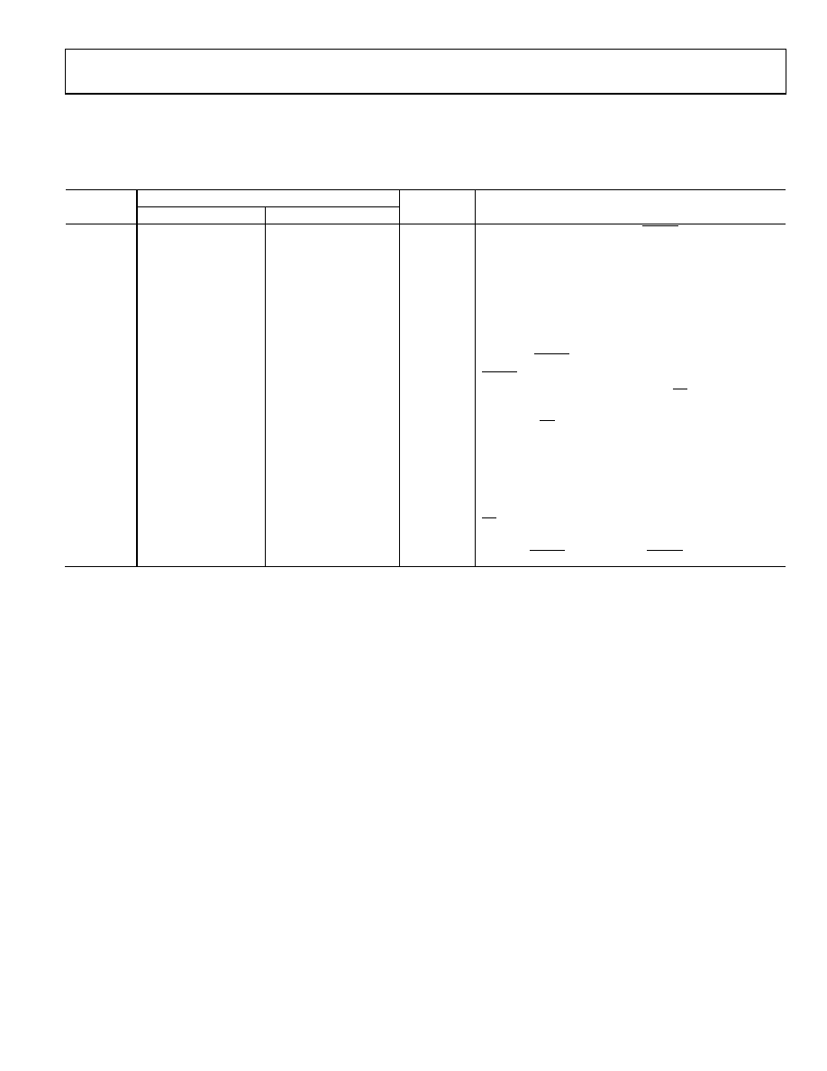
TIMING SPECIFICATIONS
AVCC = DVCC = 4.75 V to 5.25 V, VDD = 11.5 V to 16.5 V, VSS = 16.5 V to 11.5 V, VDRIVE = 2.7 V to 5.25 V, TA = 40°C to +85°C,
unless otherwise noted.1
Table 4.
Parameter
Limit at T
MIN, TMAX
Unit
Test Conditions/Comments
2.7 V ≤ V
DRIVE < 4.75 V
4.75 V ≤ V
DRIVE ≤ 5.25 V
t
CONVERT
Conversion time, internal clock; CNVST falling edge to
BUSY falling edge
680
ns max
AD7367
610
ns max
AD7366
f
SCLK
10
kHz min
Frequency of serial read clock
35
48
MHz max
t
QUIET
30
ns min
Minimum quiet time required between the end of serial
read and the start of the next conversion
t
1
10
ns min
Minimum CNVST low pulse
t
2
40
ns min
CNVST falling edge to BUSY rising edge
t
3
0
ns min
BUSY falling edge to MSB, valid when CS is low for t4 prior
to BUSY going low
t
4
10
ns max
Delay from CS falling edge until Pin 1 (DOUTA) and Pin 23
(D
OUTB) are three-state disabled
20
14
ns max
Data access time after SCLK falling edge
t
6
7
ns min
SCLK to data valid hold time
t
7
0.3 × t
SCLK
0.3 × t
SCLK
ns min
SCLK low pulse width
t
8
0.3 × t
SCLK
0.3 × t
SCLK
ns min
SCLK high pulse width
t
9
10
ns max
CS rising edge to DOUTA, DOUTB, high impedance
t
POWER-UP
70
s max
Power-up time from shutdown mode; time required
between CNVST rising edge and CNVST falling edge
1 Sample tested during initial release to ensure compliance. All input signals are specified with t
R = tF = 5 ns (10% to 90% of VDRIVE) and timed from a voltage level of 1.6 V.
All timing specifications are with a 25 pF load capacitance. With a load capacitance greater than 25 pF, a digital buffer or latch must be used. See the Terminology
section, Figure 25, and Figure 26.
2 The time required for the output to cross is 0.4 V or 2.4 V.
相关PDF资料 |
PDF描述 |
|---|---|
| AD7394ARZ | IC DAC 12BIT SERIAL 3V 14SOIC |
| AD7398BR | IC DAC 12BIT QUAD SRL 16-SOIC |
| AD7401AYRWZ-RL | IC MODULATOR SIGMA-DELTA 16SOIC |
| AD7401YRWZ | IC MODULATOR SIGMA-DELTA 16SOIC |
| AD7450ABRT-R2 | IC ADC 12BIT W/DIFF INP SOT-23-8 |
相关代理商/技术参数 |
参数描述 |
|---|---|
| AD736AK | 制造商:Analog Devices 功能描述: |
| AD736AQ | 功能描述:IC TRUE RMS/DC CONV LP 8-CDIP RoHS:否 类别:集成电路 (IC) >> PMIC - RMS 至 DC 转换器 系列:- 标准包装:46 系列:- 电流 - 电源:1.2mA 电源电压:±18 V,36 V 安装类型:表面贴装 封装/外壳:16-SOIC(0.295",7.50mm 宽) 供应商设备封装:16-SOIC W 包装:管件 |
| AD736AR | 制造商:Analog Devices 功能描述:True RMS to DC Converter 8-Pin SOIC N |
| AD736AR-REEL | 功能描述:IC TRUE RMS/DC CONV LP 8-SOIC TR RoHS:否 类别:集成电路 (IC) >> PMIC - RMS 至 DC 转换器 系列:- 标准包装:46 系列:- 电流 - 电源:1.2mA 电源电压:±18 V,36 V 安装类型:表面贴装 封装/外壳:16-SOIC(0.295",7.50mm 宽) 供应商设备封装:16-SOIC W 包装:管件 |
| AD736AR-REEL7 | 功能描述:IC TRUE RMS/DC CONV LP 8-SOIC TR RoHS:否 类别:集成电路 (IC) >> PMIC - RMS 至 DC 转换器 系列:- 标准包装:46 系列:- 电流 - 电源:1.2mA 电源电压:±18 V,36 V 安装类型:表面贴装 封装/外壳:16-SOIC(0.295",7.50mm 宽) 供应商设备封装:16-SOIC W 包装:管件 |
发布紧急采购,3分钟左右您将得到回复。