- 您现在的位置:买卖IC网 > PDF目录8671 > AD7392ARZ-REEL (Analog Devices Inc)IC DAC 12BIT PARALLEL 3V 20SOIC PDF资料下载
参数资料
| 型号: | AD7392ARZ-REEL |
| 厂商: | Analog Devices Inc |
| 文件页数: | 4/20页 |
| 文件大小: | 0K |
| 描述: | IC DAC 12BIT PARALLEL 3V 20SOIC |
| 产品培训模块: | Data Converter Fundamentals DAC Architectures |
| 标准包装: | 1,000 |
| 设置时间: | 60µs |
| 位数: | 12 |
| 数据接口: | 并联 |
| 转换器数目: | 1 |
| 电压电源: | 单电源 |
| 功率耗散(最大): | 500µW |
| 工作温度: | -40°C ~ 85°C |
| 安装类型: | 表面贴装 |
| 封装/外壳: | 20-SOIC(0.295",7.50mm 宽) |
| 供应商设备封装: | 20-SOIC W |
| 包装: | 带卷 (TR) |
| 输出数目和类型: | 1 电压,单极;1 电压,双极 |
| 采样率(每秒): | 17k |
AD7392/AD7393
Rev. C | Page 12 of 20
THEORY OF OPERATION
The AD7392/AD7393 comprise a set of pin-compatible, 12-/10-
bit digital-to-analog converters (DACs). These single-supply
operation devices consume less than 100 μA of current while
operating from 2.7 V to 5.5 V power supplies, making them
ideal for battery-operated applications. They contain a voltage-
switched, 12-/10-bit, laser-trimmed DAC; rail-to-rail output op
amps; and a parallel input DAC register. The external reference
input has constant input resistance independent of the digital
code setting of the DAC. In addition, the reference input can be
tied to the same supply voltage as VDD, resulting in a maximum
output voltage span of 0 V to VDD. The parallel data interface
consists of a CS write strobe and 12 data bits (D0 to D11) if
utilizing the AD7392 or 10 data bits (D0 to D9) if utilizing
the AD7393. An RS pin is available to reset the DAC register to
zero scale. This function is useful for power-on reset or system
failure recovery to a known state. Additional power savings are
accomplished by activating the SHDN pin, resulting in a 1.5 μA
maximum consumption sleep mode. While the supply voltage is
on, data is retained in the DAC register to reset the DAC output
when the part is taken out of shutdown (SHDN = 1).
DIGITAL-TO-ANALOG CONVERTERS
The voltage switched R-2R DAC generates an output voltage
that depends on the external reference voltage connected to
the VREF pin according to Equation 1.
N
REF
OUT
D
V
2
×
=
(1)
where:
D
is the decimal data-word loaded into the DAC register.
N
is the number of bits of DAC resolution.
If the 10-bit AD7393 uses a 2.5 V reference, Equation 1
becomes
1024
5
.
2
D
V
OUT
×
=
(2)
Using Equation 2, the nominal midscale voltage at VOUT is
1.25 V, for D = 512; full-scale voltage is 2.497 V. The LSB
step size is 2.5 × 1/1024 = 0.0024 V.
If the 12-bit AD7392 uses a 5.0 V reference, Equation 1
becomes
4096
D
V
REF
OUT
×
=
(3)
Using Equation 3, the AD7392 provides a nominal midscale volt-
age of 2.50 V (for D = 2048) and a full-scale VOUT of 4.998 V.
The LSB step size is 5.0 × 1/4096 = 0.0012 V.
AMPLIFIER SECTION
The internal DACs output is buffered by a low power consump-
tion precision amplifier. The op amp has a 60 μs typical settling
time to 0.1% of full scale. There are slight differences in settling
time for negative slew signals vs. positive. Also, negative tran-
sition settling time to within the last 6 LSBs of 0 V has an extended
settling time. The rail-to-rail output stage of this amplifier has
been designed to provide precision performance while operating
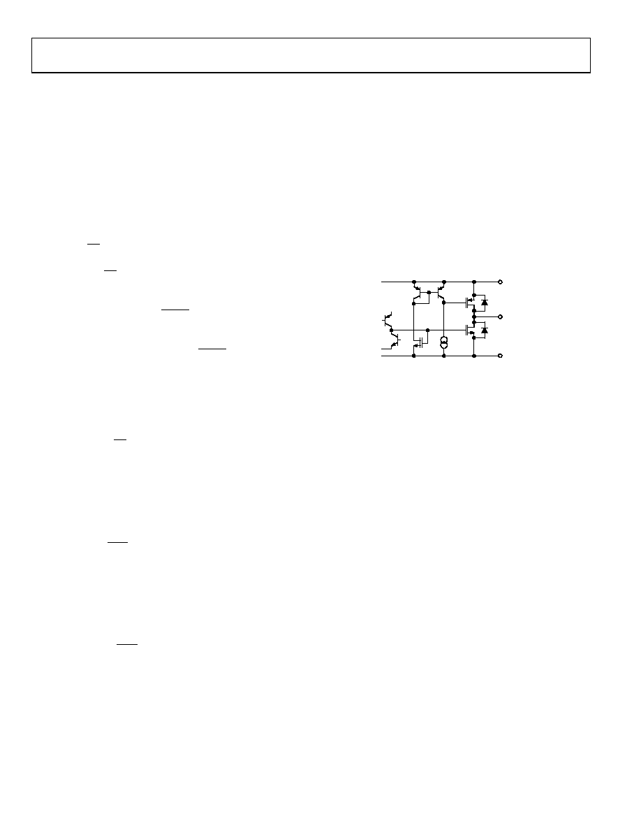
near either power supply. Figure 27 shows an equivalent output
schematic of the rail-to-rail amplifier with its N-channel pull-
down FETs that pull an output load directly to GND. The
output sourcing current is provided by a P-channel, pull-up
device that can source current-to-GND terminated loads.
01
12
1-
0
28
P-CH
N-CH
VDD
VOUT
AGND
Figure 27. Equivalent Analog Output Circuit
The rail-to-rail output stage provides ±1 mA of output current.
The N-channel output pull-down MOSFET, shown in Figure 27,
has a 35 Ω on resistance that sets the sink current capability
near ground. In addition to resistive load driving capability, the
amplifier also has been carefully designed and characterized for
up to 100 pF capacitive load driving capability.
REFERENCE INPUT
The reference input terminal has a constant input resistance
independent of digital code, which results in reduced glitches
on the external reference voltage source. The high 2.5 MΩ input
resistance minimizes power dissipation within the AD7392/
AD7393 DACs. The VREF input accepts input voltages ranging
from ground to the positive supply voltage VDD. One of the
simplest applications for saving an external reference voltage
source is connecting the REF terminal to the positive VDD
supply. This connection results in a rail-to-rail voltage output
span maximizing the programmed range. The reference input
accepts ac signals as long as they stay within the 0 V < VREF <
VDD supply voltage range. The reference bandwidth and integral
nonlinearity error performance are plotted in Figure 20 and
Figure 21. The ratiometric reference feature makes the AD7392/
AD7393 an ideal companion to ratiometric analog-to-digital
converters (ADCs) such as the AD7896.
相关PDF资料 |
PDF描述 |
|---|---|
| VI-J4P-MY | CONVERTER MOD DC/DC 13.8V 50W |
| VI-J4M-MY | CONVERTER MOD DC/DC 10V 50W |
| VI-JWH-MX-B1 | CONVERTER MOD DC/DC 52V 75W |
| SY10EP11UKC | IC CLOCK BUFFER 1:2 3GHZ 8-MSOP |
| VI-J73-MX-B1 | CONVERTER MOD DC/DC 24V 75W |
相关代理商/技术参数 |
参数描述 |
|---|---|
| AD7393 | 制造商:AD 制造商全称:Analog Devices 功能描述:+3 V, Parallel Input Micropower 10- and 12-Bit DACs |
| AD7393AN | 制造商:Rochester Electronics LLC 功能描述:10-BIT +3V TO +5V UPOWER DAC, PARALLEL - Bulk 制造商:Analog Devices 功能描述:CONVERTOR DA ((NW)) 制造商:Analog Devices Inc. 功能描述:3 V, Parallel Input 10-Bit DACs |
| AD7393AR | 制造商:Analog Devices 功能描述:DAC 1-CH R-2R 10-bit 20-Pin SOIC W 制造商:Rochester Electronics LLC 功能描述:10-BIT +3V TO +5V UPOWER DAC, PARALLEL - Bulk 制造商:Analog Devices 功能描述:PARALLEL, WORD INPUT LOADING, 70 us SETTLING TIME, 10-BIT DAC, PDSO20 |
| AD7393ARU | 制造商:AD 制造商全称:Analog Devices 功能描述:+3 V, Parallel Input Micropower 10- and 12-Bit DACs |
| ad7393aru-reel | 制造商:Rochester Electronics LLC 功能描述:10-BIT +3V TO +5V UPOWER DAC, PARALLEL - Tape and Reel 制造商:Analog Devices 功能描述: |
发布紧急采购,3分钟左右您将得到回复。