- 您现在的位置:买卖IC网 > PDF目录8671 > AD7392ARZ-REEL (Analog Devices Inc)IC DAC 12BIT PARALLEL 3V 20SOIC PDF资料下载
参数资料
| 型号: | AD7392ARZ-REEL |
| 厂商: | Analog Devices Inc |
| 文件页数: | 5/20页 |
| 文件大小: | 0K |
| 描述: | IC DAC 12BIT PARALLEL 3V 20SOIC |
| 产品培训模块: | Data Converter Fundamentals DAC Architectures |
| 标准包装: | 1,000 |
| 设置时间: | 60µs |
| 位数: | 12 |
| 数据接口: | 并联 |
| 转换器数目: | 1 |
| 电压电源: | 单电源 |
| 功率耗散(最大): | 500µW |
| 工作温度: | -40°C ~ 85°C |
| 安装类型: | 表面贴装 |
| 封装/外壳: | 20-SOIC(0.295",7.50mm 宽) |
| 供应商设备封装: | 20-SOIC W |
| 包装: | 带卷 (TR) |
| 输出数目和类型: | 1 电压,单极;1 电压,双极 |
| 采样率(每秒): | 17k |
AD7392/AD7393
Rev. C | Page 13 of 20
POWER SUPPLY
The very low power consumption of the AD7392/AD7393 is
a direct result of a circuit design that optimizes the CBCMOS
process. By using the low power characteristics of CMOS for the
logic and the low noise, tight-matching of the complementary
bipolar transistors, excellent analog accuracy is achieved. One
advantage of the rail-to-rail output amplifiers used in the AD7392/
AD7393 is the wide range of usable supply voltage. The part is
fully specified and tested for operation from 2.7 V to 5.5 V.
01
12
1-
029
5V
POWER SUPPLY
5V
RETURN
FERRITE BEAD:
2 TURNS, FAIR-RITE
#2677006301
TTL/CMOS
LOGIC
CIRCUITS
+ 100F
ELECT.
+10F TO 22F
TANT.
+ 0.1F
CER.
Figure 28. Use Separate Traces to Reduce Power Supply Noise
Whether or not a separate power supply trace is available, gen-
erous supply bypassing reduces supply line induced errors. Local
supply bypassing, consisting of a 10 μF tantalum electrolytic in
parallel with a 0.1 μF ceramic capacitor, is recommended for all
applications (see Figure 29).
0
112
1-
03
0
VOUT
CS
1
20
19
17, 18
4
3
2
C
*
RS
D0 TO D11
2.7V TO 5.5V
VDD
VREF
GND
SHDN
AD7392
OR
AD7393
0.1F
10F
+
* OPTIONAL EXTERNAL
REFERENCE BYPASS
Figure 29. Recommended Supply Bypassing for the AD7392/AD7393
INPUT LOGIC LEVELS
All digital inputs are protected with a Zener-type ESD protection
structure that allows logic input voltages to exceed the VDD supply
voltage (see Figure 30). This feature is useful if the user is driving
one or more of the digital inputs with a 5 V CMOS logic input
voltage level while operating the AD7392/AD7393 on a 3 V
power supply. If this interface is used, make sure that the VOL
of the 5 V CMOS meets the VIL input requirement of the AD7392/
AD7393 operating at 3 V. See Figure 12 for a graph of digital
logic input threshold vs. operating VDD supply voltage.
01
12
1-
03
1
VDD
LOGIC
IN
GND
1k
Figure 30. Equivalent Digital Input ESD Protection
To minimize power dissipation from input logic levels that
are near the VIH and VIL logic input voltage specifications, a
Schmitt-trigger design was used that minimizes the input
buffer current consumption compared to traditional CMOS
input stages. Figure 11 is a plot of supply current vs. incremental
input voltage, showing that negligible current consumption
takes place when logic levels are in their quiescent state. The
normal crossover current still occurs during logic transitions.
A secondary advantage of this Schmitt trigger is the prevention
of false triggers that would occur with slow moving logic transi-
tions when a standard CMOS logic interface or opto-isolators
are used. Logic inputs D11 to D0, CS, RS, and SHDN all contain
the Schmitt-trigger circuits.
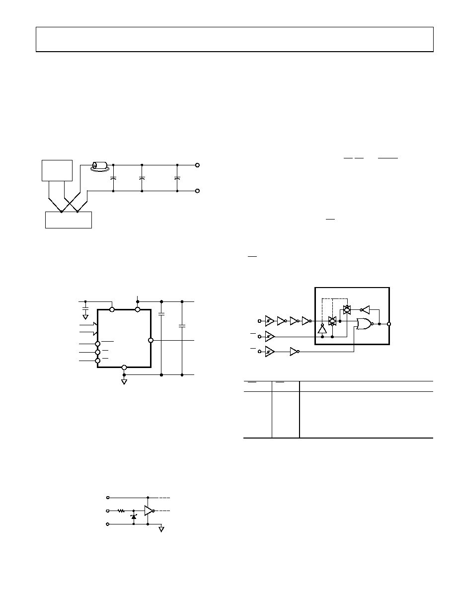
DIGITAL INTERFACE
The AD7392/AD7393 have a parallel data input. A functional
block diagram of the digital section is shown in Figure 31,
while Table 6 contains the truth table for the logic control
inputs. The chip select pin (CS) controls loading of data from
the data inputs on Pin D11 to Pin D0. This active low input
places the input register into a transparent state allowing the
data inputs to directly change the DAC ladder values. When
CS returns to logic high within the data setup-and-hold time
specifications, the new value of data in the input register are
latched. See Table 6 for a complete listing of conditions.
01
12
1-
0
05
Dx
CS
RS
TO
INTERNAL
DAC SWITCHES
1 OF 12 LATCHES
OF THE
DAC REGISTER
Figure 31. Digital Control Logic
Table 6. Control Logic Truth Table
CS
RS
DAC Register Function
H
Latched
L
H
Transparent
H
Latched with new data
L
Loaded with all zeros
H
Latched all zeros
1
↑ = Positive logic transition.
2 X = Don’t care.
相关PDF资料 |
PDF描述 |
|---|---|
| VI-J4P-MY | CONVERTER MOD DC/DC 13.8V 50W |
| VI-J4M-MY | CONVERTER MOD DC/DC 10V 50W |
| VI-JWH-MX-B1 | CONVERTER MOD DC/DC 52V 75W |
| SY10EP11UKC | IC CLOCK BUFFER 1:2 3GHZ 8-MSOP |
| VI-J73-MX-B1 | CONVERTER MOD DC/DC 24V 75W |
相关代理商/技术参数 |
参数描述 |
|---|---|
| AD7393 | 制造商:AD 制造商全称:Analog Devices 功能描述:+3 V, Parallel Input Micropower 10- and 12-Bit DACs |
| AD7393AN | 制造商:Rochester Electronics LLC 功能描述:10-BIT +3V TO +5V UPOWER DAC, PARALLEL - Bulk 制造商:Analog Devices 功能描述:CONVERTOR DA ((NW)) 制造商:Analog Devices Inc. 功能描述:3 V, Parallel Input 10-Bit DACs |
| AD7393AR | 制造商:Analog Devices 功能描述:DAC 1-CH R-2R 10-bit 20-Pin SOIC W 制造商:Rochester Electronics LLC 功能描述:10-BIT +3V TO +5V UPOWER DAC, PARALLEL - Bulk 制造商:Analog Devices 功能描述:PARALLEL, WORD INPUT LOADING, 70 us SETTLING TIME, 10-BIT DAC, PDSO20 |
| AD7393ARU | 制造商:AD 制造商全称:Analog Devices 功能描述:+3 V, Parallel Input Micropower 10- and 12-Bit DACs |
| ad7393aru-reel | 制造商:Rochester Electronics LLC 功能描述:10-BIT +3V TO +5V UPOWER DAC, PARALLEL - Tape and Reel 制造商:Analog Devices 功能描述: |
发布紧急采购,3分钟左右您将得到回复。