参数资料
| 型号: | AD7398BRUZ |
| 厂商: | Analog Devices Inc |
| 文件页数: | 6/24页 |
| 文件大小: | 0K |
| 描述: | IC DAC 12BIT QUAD SRL-IN 16TSSOP |
| 产品培训模块: | Data Converter Fundamentals DAC Architectures |
| 标准包装: | 1 |
| 设置时间: | 6µs |
| 位数: | 12 |
| 数据接口: | 串行,SPI? |
| 转换器数目: | 4 |
| 电压电源: | 双 ± |
| 功率耗散(最大): | 16mW |
| 工作温度: | -40°C ~ 125°C |
| 安装类型: | 表面贴装 |
| 封装/外壳: | 16-TSSOP(0.173",4.40mm 宽) |
| 供应商设备封装: | 16-TSSOP |
| 包装: | 管件 |
| 输出数目和类型: | 4 电压,单极 |
| 采样率(每秒): | 167k |
| 产品目录页面: | 784 (CN2011-ZH PDF) |
AD7398/AD7399
Rev. C | Page 14 of 24
THEORY OF OPERATION
0
21
79
-0
25
VREFA
VDD
VREFB VREFC VREFD
DAC A
DAC
REGISTER
INPUT
REGISTER
VOUTA
DAC B
DAC
REGISTER
INPUT
REGISTER
VOUTB
DAC C
DAC
REGISTER
INPUT
REGISTER
VOUTC
DAC D
DAC
REGISTER
INPUT
REGISTER
VOUTD
SERIAL
REGISTER
CLK
SDI
CS
AD7398/AD7399
POWER
ON RESET
VSS
GND
RS
LDAC
ADDRESS
DECODE
4
12/10
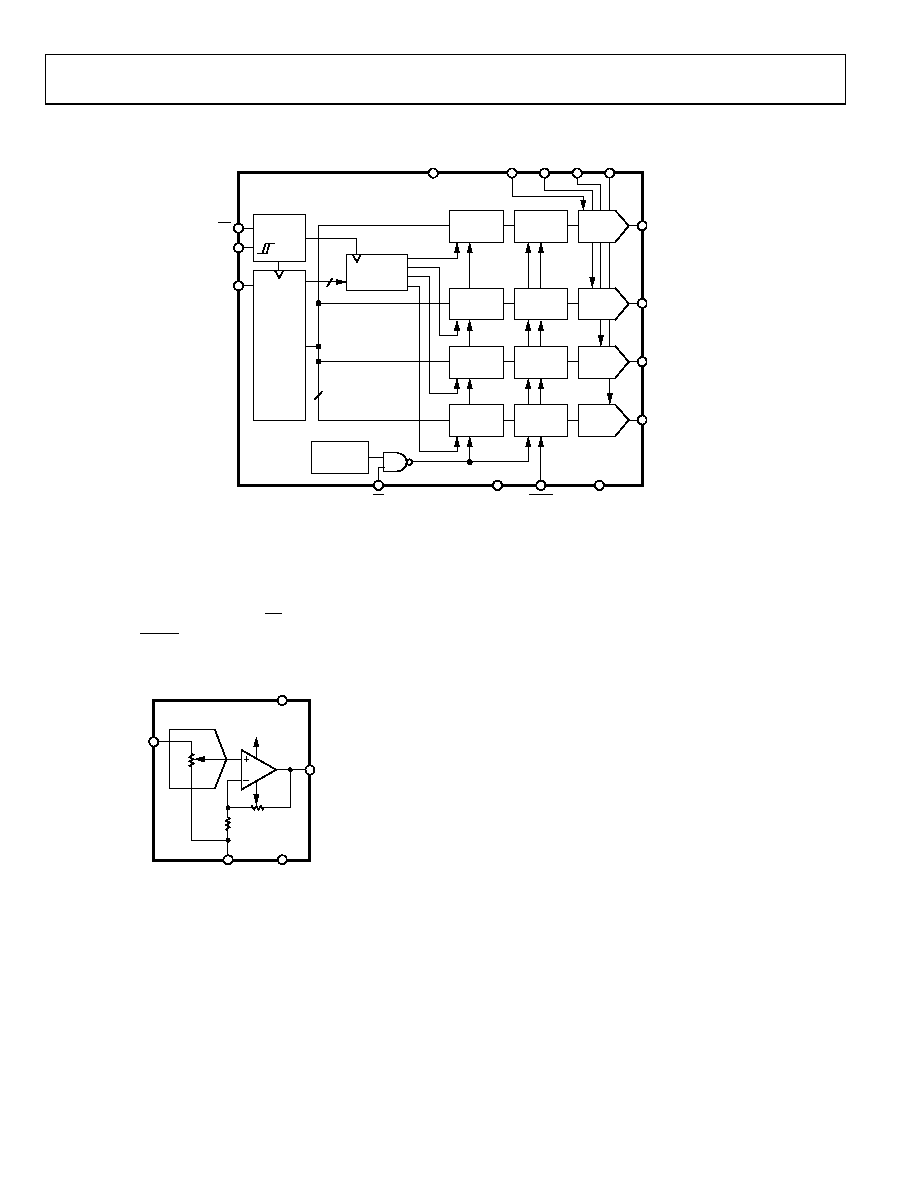
Figure 25. Simplified Block Diagram
The AD7398/AD7399 contain four 12-bit and 10-bit,
respectively, voltage output, digital-to-analog converters. Each
DAC has its own independent multiplying reference input. Both
the AD7398 and AD7399 use a 3-wire, SPI-compatible serial
data interface, with an asynchronous RS pin for zero-scale reset.
In addition, an LDAC strobe enables four-channel simultaneous
updates for hardware-synchronized output voltage changes.
02
17
9-
02
6
AD7398/AD7399
VOUTA
VREF
GND
VSS
VDD
R
Figure 26. Simplified DAC Channel
DAC OPERATION
The internal R-2R ladder of the AD7398/AD7399 operates in
the voltage switching mode, maintaining an output voltage that
is the same polarity as the input reference voltage. A proprietary
scaling technique is used to attenuate the input reference voltage in
the DAC. The output buffer amplifies the internal DAC output to
achieve a VREF to VOUT gain of unity.
The nominal DAC output voltage is determined by the
externally applied VREF and the digital data (D) as
VOUT = VREF × D/4096 (For AD7398)
(1)
VOUT = VREF × D/1024 (For AD7399)
(2)
where:
D is the 12-bit or 10-bit decimal equivalent of the data word.
VREF is the externally applied reference voltage.
In order to maintain good analog performance, the user should
bypass power supplies with 0.01 μF ceramic capacitors (mount
them close to the supply pins) and 1 μF to 10 μF tantalum
capacitors in parallel. In addition, clean power supplies with low
ripple voltage capability should be used. Switching power supplies
can be used for this application, but beware of its higher ripple
voltage and PSS frequency-dependent characteristics. It is also
best to supply power to the AD7398/AD7399 from the system’s
analog supply voltages. Do not use the digital 5 V supply.
The reference input resistance is code dependent, exhibiting
worst case 35 kΩ for AD7398 when the DAC is loaded with
alternating codes 010101010101. Similarly, the reference input
resistance is 40 kΩ for AD7399 when the DAC is loaded with
0101010101.
相关PDF资料 |
PDF描述 |
|---|---|
| MS27467T25F4SD | CONN PLUG 56POS STRAIGHT W/SCKT |
| VI-24Y-MU-F2 | CONVERTER MOD DC/DC 3.3V 132W |
| VI-J0Z-MZ-F3 | CONVERTER MOD DC/DC 2V 10W |
| VI-J0Z-MZ-F2 | CONVERTER MOD DC/DC 2V 10W |
| TXB0104RUTR | IC VOLT-LEVEL TRANSLATOR 12UQFN |
相关代理商/技术参数 |
参数描述 |
|---|---|
| AD7398BRUZ | 制造商:Analog Devices 功能描述:IC, DAC, 12BIT, 167KSPS, TSSOP-16 |
| AD7398BRUZ-REEL7 | 功能描述:IC DAC 12BIT QUAD SERIAL 16TSSOP RoHS:是 类别:集成电路 (IC) >> 数据采集 - 数模转换器 系列:- 标准包装:47 系列:- 设置时间:2µs 位数:14 数据接口:并联 转换器数目:1 电压电源:单电源 功率耗散(最大):55µW 工作温度:-40°C ~ 85°C 安装类型:表面贴装 封装/外壳:28-SSOP(0.209",5.30mm 宽) 供应商设备封装:28-SSOP 包装:管件 输出数目和类型:1 电流,单极;1 电流,双极 采样率(每秒):* |
| AD7398BRZ | 功能描述:IC DAC 12BIT QUAD SRL 16-SOIC RoHS:是 类别:集成电路 (IC) >> 数据采集 - 数模转换器 系列:- 标准包装:1 系列:- 设置时间:4.5µs 位数:12 数据接口:串行,SPI? 转换器数目:1 电压电源:单电源 功率耗散(最大):- 工作温度:-40°C ~ 125°C 安装类型:表面贴装 封装/外壳:8-SOIC(0.154",3.90mm 宽) 供应商设备封装:8-SOICN 包装:剪切带 (CT) 输出数目和类型:1 电压,单极;1 电压,双极 采样率(每秒):* 其它名称:MCP4921T-E/SNCTMCP4921T-E/SNRCTMCP4921T-E/SNRCT-ND |
| AD7398BRZ-REEL | 功能描述:IC DAC 12BIT QUAD SERIAL 16SOIC RoHS:是 类别:集成电路 (IC) >> 数据采集 - 数模转换器 系列:- 标准包装:47 系列:- 设置时间:2µs 位数:14 数据接口:并联 转换器数目:1 电压电源:单电源 功率耗散(最大):55µW 工作温度:-40°C ~ 85°C 安装类型:表面贴装 封装/外壳:28-SSOP(0.209",5.30mm 宽) 供应商设备封装:28-SSOP 包装:管件 输出数目和类型:1 电流,单极;1 电流,双极 采样率(每秒):* |
| AD7398BRZ-REEL7 | 制造商:AD 制造商全称:Analog Devices 功能描述:Quad, Serial-Input 12-Bit/10-Bit DACs |
发布紧急采购,3分钟左右您将得到回复。