参数资料
| 型号: | AD7398BRUZ |
| 厂商: | Analog Devices Inc |
| 文件页数: | 7/24页 |
| 文件大小: | 0K |
| 描述: | IC DAC 12BIT QUAD SRL-IN 16TSSOP |
| 产品培训模块: | Data Converter Fundamentals DAC Architectures |
| 标准包装: | 1 |
| 设置时间: | 6µs |
| 位数: | 12 |
| 数据接口: | 串行,SPI? |
| 转换器数目: | 4 |
| 电压电源: | 双 ± |
| 功率耗散(最大): | 16mW |
| 工作温度: | -40°C ~ 125°C |
| 安装类型: | 表面贴装 |
| 封装/外壳: | 16-TSSOP(0.173",4.40mm 宽) |
| 供应商设备封装: | 16-TSSOP |
| 包装: | 管件 |
| 输出数目和类型: | 4 电压,单极 |
| 采样率(每秒): | 167k |
| 产品目录页面: | 784 (CN2011-ZH PDF) |
AD7398/AD7399
Rev. C | Page 15 of 24
OPERATION WITH VREF EQUAL TO THE SUPPLY
The AD7398/AD7399 are designed to approach the full output
voltage swing from ground to VDD or VSS. The maximum output
swing is achieved when the corresponding VREF input pin is tied
to the same power supply. This power supply should be low noise
and low ripple, preferably operated by a suitable reference voltage
source such as ADR292 or REF02. The output swing is limited
by the internal buffer offset voltage and the output drive current
capability of the output stage. Users should at least budget the VZSE
offset voltage as the closest the output voltage can get to either
supply voltage under a no load condition. Under a loaded output,
degrade the headroom by a factor of 2 mV per 1 mA of load
current. Also note that the internal op amp has an offset voltage
so that the first eight codes of AD7398 may not respond at the
supply voltage or at ground until the internal DAC voltage
exceeds the offset voltage of the output buffers. Similarly, the first
two codes of AD7399 should not be used.
POWER SUPPLY SEQUENCING
VDD/VSS of AD7398/AD7399 should be powered from the system
analog supplies. The external reference input can be supplied from
the same supply to avoid a possible latch-up when the reference is
powered on prior to VDD/VSS, or powered off subsequent to
VDD/VSS. If VDD/VSS and VREF have separate power sources, ensure
the power-up sequence is GND, VDD, VSS, VREF/digital input/digital
output. The reverse sequence applies to the power-down sequence.
The order of VREF and digital input/digital output is not important.
In addition, VREF pins of the unused DACs should be connected to
GND or some other power sources to ensure a similar power-
up/power-down sequence.
PROGRAMMABLE POWER SHUTDOWN
The two MSBs of the serial input register, SA and SD, are used
to program various shutdown modes. If SA is set to Logic 1, all
DACs are placed in shutdown mode. If SA = 0 and SD = 1, a
corresponding DAC is shutdown addressed by Bit A0 and
Bit A1 (see the Input Registers section).
WORST CASE ACCURACY
Assuming a perfect reference, the worst-case output voltage can
be calculated from the following equation:
INL
V
D
V
ZSE
FSE
REF
N
OUT
2
(3)
where:
D = decimal code loaded to DAC ranges 0 ≤ D ≤ 2N–1.
N = number of bits.
VREF = applied reference voltage.
VFSE = full-scale error in volts.
VZSE = zero-scale error in volts.
INL = integral nonlinearity in volts. INL is 0 at full scale or zero
scale.
SERIAL DATA INTERFACE
The AD7398/AD7399 uses a 3-wire (CS, SDI, CLK) SPI-
compatible serial data interface. Serial data of the AD7398 and
AD7399 is clocked into the serial input register in a 16-bit and 14-
bit data-word format, respectively. MSBs are loaded first. The Input
Registers section defines the 16 data-word bits for AD7398 and the
14 data-word bits for the AD7399. Data is placed on the SDI pin,
and clocked into the register on the positive clock edge of CLK,
subject to the data setup and data hold time requirements specified
in the Specifications section. Data can only be clocked in while the
CS chip select pin is active low. For the AD7398, only the last 16
bits clocked into the serial register are interrogated when the CS pin
returns to the logic high state, and extra data bits are ignored. For
the AD7399, only the last 14 bits clocked into the serial register are
interrogated when the CS pin returns to the logic high state.
Because most microcontrollers output serial data is in eight-bit
bytes, two right-justified data bytes can be written to the AD7398
and AD7399. Keeping the CS line low between the first and second
byte transfers results in a successful serial register update.
Once the data is properly aligned in the shift register, the positive
edge of the CS initiates the transfer of new data to the target DAC
register, determined by the decoding of Address Bit A1 and
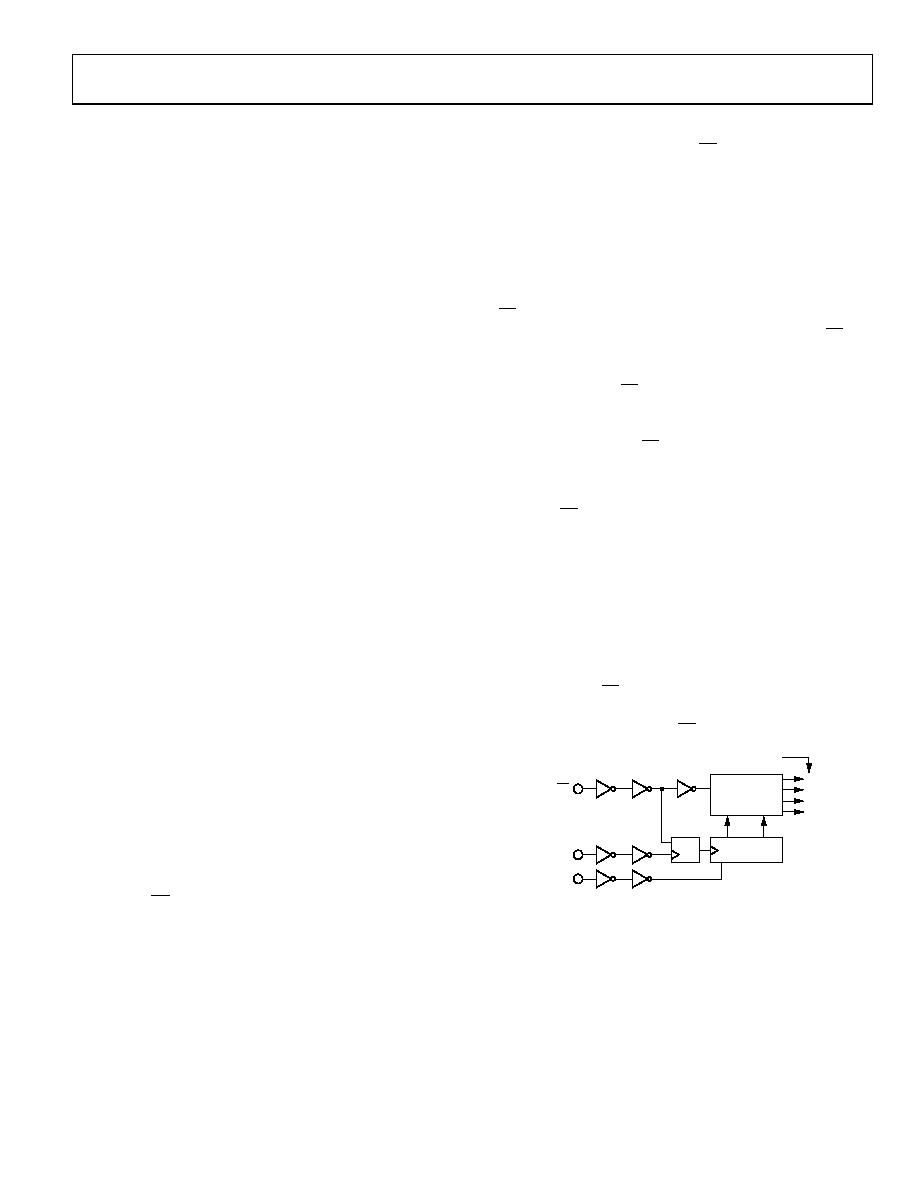
Registers section, and Figure 4 (with a 14-bit exception) define the
characteristics of the serial interface. Figure 27 and Figure 28 show
the equivalent logic interface for the key digital control pins for
AD7398 and AD7399.
An asynchronous RS provides hardware control reset to zero-
code state over the preset function and DAC register loading. If
this function is not needed, the RS pin can be tied to logic high.
02
17
9-
02
7
EN
CLK
SDI
SHIFT
REGISTER
ADDRESS
DECODER
A
B
C
D
CS
TO INPUT REGISTER
Figure 27. Equivalent Logic Interface
相关PDF资料 |
PDF描述 |
|---|---|
| MS27467T25F4SD | CONN PLUG 56POS STRAIGHT W/SCKT |
| VI-24Y-MU-F2 | CONVERTER MOD DC/DC 3.3V 132W |
| VI-J0Z-MZ-F3 | CONVERTER MOD DC/DC 2V 10W |
| VI-J0Z-MZ-F2 | CONVERTER MOD DC/DC 2V 10W |
| TXB0104RUTR | IC VOLT-LEVEL TRANSLATOR 12UQFN |
相关代理商/技术参数 |
参数描述 |
|---|---|
| AD7398BRUZ | 制造商:Analog Devices 功能描述:IC, DAC, 12BIT, 167KSPS, TSSOP-16 |
| AD7398BRUZ-REEL7 | 功能描述:IC DAC 12BIT QUAD SERIAL 16TSSOP RoHS:是 类别:集成电路 (IC) >> 数据采集 - 数模转换器 系列:- 标准包装:47 系列:- 设置时间:2µs 位数:14 数据接口:并联 转换器数目:1 电压电源:单电源 功率耗散(最大):55µW 工作温度:-40°C ~ 85°C 安装类型:表面贴装 封装/外壳:28-SSOP(0.209",5.30mm 宽) 供应商设备封装:28-SSOP 包装:管件 输出数目和类型:1 电流,单极;1 电流,双极 采样率(每秒):* |
| AD7398BRZ | 功能描述:IC DAC 12BIT QUAD SRL 16-SOIC RoHS:是 类别:集成电路 (IC) >> 数据采集 - 数模转换器 系列:- 标准包装:1 系列:- 设置时间:4.5µs 位数:12 数据接口:串行,SPI? 转换器数目:1 电压电源:单电源 功率耗散(最大):- 工作温度:-40°C ~ 125°C 安装类型:表面贴装 封装/外壳:8-SOIC(0.154",3.90mm 宽) 供应商设备封装:8-SOICN 包装:剪切带 (CT) 输出数目和类型:1 电压,单极;1 电压,双极 采样率(每秒):* 其它名称:MCP4921T-E/SNCTMCP4921T-E/SNRCTMCP4921T-E/SNRCT-ND |
| AD7398BRZ-REEL | 功能描述:IC DAC 12BIT QUAD SERIAL 16SOIC RoHS:是 类别:集成电路 (IC) >> 数据采集 - 数模转换器 系列:- 标准包装:47 系列:- 设置时间:2µs 位数:14 数据接口:并联 转换器数目:1 电压电源:单电源 功率耗散(最大):55µW 工作温度:-40°C ~ 85°C 安装类型:表面贴装 封装/外壳:28-SSOP(0.209",5.30mm 宽) 供应商设备封装:28-SSOP 包装:管件 输出数目和类型:1 电流,单极;1 电流,双极 采样率(每秒):* |
| AD7398BRZ-REEL7 | 制造商:AD 制造商全称:Analog Devices 功能描述:Quad, Serial-Input 12-Bit/10-Bit DACs |
发布紧急采购,3分钟左右您将得到回复。